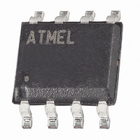
AT25DF321A-SH-T Atmel, AT25DF321A-SH-T Datasheet - Page 17

AT25DF321A-SH-T
Manufacturer Part Number
AT25DF321A-SH-T
Description
IC FLASH 32MBIT 100MHZ 8SOIC
Manufacturer
Atmel
Datasheet
1.AT25DF321A-SH-T.pdf
(51 pages)
Specifications of AT25DF321A-SH-T
Format - Memory
FLASH
Memory Type
DataFLASH
Memory Size
32M (16384 pages x 256 Bytes)
Speed
100MHz
Interface
SPI, RapidS
Voltage - Supply
2.7 V ~ 3.6 V
Operating Temperature
-40°C ~ 85°C
Package / Case
8-SOIC (5.3mm Width), 8-SOP, 8-SOEIAJ
Density
32Mb
Access Time (max)
5ns
Interface Type
Serial (SPI)
Address Bus
1b
Operating Supply Voltage (typ)
3.3V
Operating Temp Range
-40C to 85C
Package Type
SOIC
Program/erase Volt (typ)
2.7 to 3.6V
Sync/async
Synchronous
Operating Temperature Classification
Industrial
Operating Supply Voltage (min)
2.7V
Operating Supply Voltage (max)
3.6V
Word Size
8b
Number Of Words
4M
Supply Current
19mA
Mounting
Surface Mount
Pin Count
8
Lead Free Status / RoHS Status
Lead free / RoHS Compliant
Available stocks
Company
Part Number
Manufacturer
Quantity
Price
Company:
Part Number:
AT25DF321A-SH-T
Manufacturer:
CYPRESS
Quantity:
1 872
Part Number:
AT25DF321A-SH-T
Manufacturer:
ATMEL/爱特梅尔
Quantity:
20 000
3686D–DFLASH–12/09
8.6
Figure 8-7.
Program/Erase Resume
The Program/Erase Resume command allows a suspended program or erase operation to be resumed and continue
programming a Flash page or erasing a Flash memory block where it left off. As with the Program/Erase Suspend
command, the Write Enable command does not need to be issued prior to the Program/Erase Resume command being
issued. Therefore, the Program/Erase Resume command operates independently of the state of the WEL bit in the Status
Register.
To perform a Program/Erase Resume, the CS pin must first be asserted and the opcode of D0h must be clocked into the
device. No address bytes need to be clocked into the device, and any data clocked in after the opcode will be ignored.
When the CS pin is deasserted, the program or erase operation currently suspended will be resumed within a time of t
The PS bit or the ES bit in the Status Register will then be reset back to the logical “0” state to indicate that the program
or erase operation is no longer suspended. In addition, the RDY/BSY bit in the Status Register will indicate that the device
is busy performing a program or erase operation. The complete opcode must be clocked into the device before the CS pin
is deasserted, and the CS pin must be deasserted on an even byte boundary (multiples of eight bits); otherwise, no
resume operation will be performed.
During a simultaneous Erase Suspend/Program Suspend condition, issuing the Program/Erase Resume command will
result in the program operation resuming first. After the program operation has been completed, the Program/Erase
Resume command must be issued again in order for the erase operation to be resumed.
While the device is busy resuming a program or erase operation, any attempts at issuing the Program/Erase Suspend
command will be ignored. Therefore, if a resumed program or erase operation needs to be subsequently suspended again,
the system must either wait the entire t
status of the RDY/BSY bit or the appropriate PS or ES bit in the Status Register to determine if the previously suspended
program or erase operation has resumed.
Figure 8-8.
SCK
SCK
SO
SO
CS
CS
SI
SI
Program/Erase Suspend
Program/Erase Resume
HIGH-IMPEDANCE
HIGH-IMPEDANCE
MSB
MSB
1
1
0
0
0
1
1
1
1
0
2
2
OPCODE
OPCODE
1
1
3
3
0
0
4
4
0
0
5
5
0
0
6
6
0
0
7
7
RES
time before issuing the Program/Erase Suspend command, or it must check the
Atmel AT25DF321A
RES
17
.


