EPCS16SI16N Altera, EPCS16SI16N Datasheet
EPCS16SI16N
Specifications of EPCS16SI16N
EPCS16SI16
Available stocks


Related parts for EPCS16SI16N


EPCS16SI16N Summary of contents
Page 1
... Altera warrants performance of its semiconductor products to current specifications in accordance with Altera’s standard warranty, but reserves the right to make changes to any products and services at any time without notice. Altera assumes no responsibility or liability arising out of the application or use of any information, product, or service described herein except as expressly agreed to in writing by Altera. Altera customers are advised to obtain the latest version of device specifications before relying on any published information and before placing orders for products or services ...
Page 2
... Notes to Table 3–1: (1) To program these devices using Altera Programming Unit or Master Programming Unit, refer to (2) The EPCS device can be re-programmed in system with Byte Blaster II download cable or an external microprocessor using SRunner. For more information about SRunner, refer to the AN418, SRunner: An Embedded Solution for EPCS For an 8-pin SOIC package, you can migrate vertically from the EPCS1 to the EPCS4 or EPCS16 because the EPCS devices are offered in the same device package ...
Page 3
... For more information about accessing memory within the serial configuration device, refer to the Active Serial Memory Interface Data Active Serial FPGA Configuration The following Altera FPGAs support Active Serial (AS) configuration scheme with serial configuration devices: ■ Arria series ■ Cyclone series ■ ...
Page 4
... Connect the FPGA MSEL[] input pins to select the AS configuration mode. For details, refer to the respective FPGA family chapter in the Configuration Handbook. (4) For more information about configuration pin I/O requirements scheme for an Altera FPGA, refer to the respective FPGA family handbook Configuration chapter. Volume 2: Configuration Handbook ...
Page 5
... Connect the FPGA MSEL[] input pins to select the AS configuration mode. For details, refer to the respective FPGA family chapter in the Configuration Handbook. (4) For more information about configuration pin I/O requirements scheme for an Altera FPGA, refer to the respective FPGA family handbook Configuration chapter. The FPGA acts as the configuration master in the configuration flow and provides the clock to the serial configuration device ...
Page 6
... Connect the FPGA MSEL[] input pins to select the PS configuration mode. For details, refer to the appropriate FPGA family chapter in the Configuration Handbook. (5) For more information about configuration pin I/O requirements scheme for an Altera FPGA, refer to the respective FPGA family handbook Configuration chapter. Volume 2: Configuration Handbook Figure 3– ...
Page 7
... Total number of 65,536 pages Bytes per page 256 bytes Table 3–3 through EPCS16, EPCS4, and EPCS1. Table 3–3. Address Range for Sectors in EPCS128 (Part Sector June 2011 Altera Corporation section. EPCS64 EPCS16 8,388,608 bytes 2,097,152 bytes (64 Mbits) (16 Mbits) 128 32 65,536 bytes ...
Page 8
... H'BBFFFF H'B7FFFF H'B3FFFF H'AFFFFF H'ABFFFF H'A7FFFF H'A3FFFF H'9FFFFF H'9BFFFF H'97FFFF H'93FFFF H'8FFFFF H'8BFFFF H'87FFFF H'83FFFF H'7FFFFF H'7BFFFF H'77FFFF H'73FFFF H'6FFFFF H'6BFFFF H'67FFFF H'63FFFF H'5FFFFF H'5BFFFF H'57FFFF H'53FFFF H'4FFFFF H'4BFFFF H'47FFFF H'43FFFF H'3FFFFF H'3BFFFF H'37FFFF H'33FFFF H'2FFFFF H'2BFFFF June 2011 Altera Corporation ...
Page 9
... Chapter 3: Serial Configuration Devices (EPCS1, EPCS4, EPCS16, EPCS64, and EPCS128) Data Sheet Serial Configuration Device Memory Access Table 3–3. Address Range for Sectors in EPCS128 (Part Sector June 2011 Altera Corporation Address Range (Byte Addresses in HEX) Start 9 H'240000 8 H'200000 7 H'1C0000 6 H'180000 5 H'140000 ...
Page 10
... H'7EFFFF H'7DFFFF H'7CFFFF H'7BFFFF H'7AFFFF H'79FFFF H'78FFFF H'77FFFF H'76FFFF H'75FFFF H'74FFFF H'73FFFF H'72FFFF H'71FFFF H'70FFFF H'6FFFFF H'6EFFFF H'6DFFFF H'6CFFFF H'6BFFFF H'6AFFFF H'69FFFF H'68FFFF H'67FFFF H'66FFFF H'65FFFF H'64FFFF H'63FFFF H'62FFFF H'61FFFF H'60FFFF H'5FFFFF H'5EFFFF H'5DFFFF H'5CFFFF H'5BFFFF H'5AFFFF June 2011 Altera Corporation ...
Page 11
... Chapter 3: Serial Configuration Devices (EPCS1, EPCS4, EPCS16, EPCS64, and EPCS128) Data Sheet Serial Configuration Device Memory Access Table 3–4. Address Range for Sectors in EPCS64 (Part Sector June 2011 Altera Corporation Address Range (Byte Addresses in HEX) Start 89 H'590000 88 H'580000 87 H'570000 86 H'560000 85 H'550000 ...
Page 12
... H'32FFFF H'31FFFF H'30FFFF H'2FFFFF H'2EFFFF H'2DFFFF H'2CFFFF H'2BFFFF H'2AFFFF H'29FFFF H'28FFFF H'27FFFF H'26FFFF H'25FFFF H'24FFFF H'23FFFF H'22FFFF H'21FFFF H'20FFFF H'1FFFFF H'1EFFFF H'1DFFFF H'1CFFFF H'1BFFFF H'1AFFFF H'19FFFF H'18FFFF H'17FFFF H'16FFFF H'15FFFF H'14FFFF H'13FFFF H'12FFFF H'11FFFF H'10FFFF H'0FFFFF H'0EFFFF June 2011 Altera Corporation ...
Page 13
... Chapter 3: Serial Configuration Devices (EPCS1, EPCS4, EPCS16, EPCS64, and EPCS128) Data Sheet Serial Configuration Device Memory Access Table 3–4. Address Range for Sectors in EPCS64 (Part Sector June 2011 Altera Corporation Address Range (Byte Addresses in HEX) Start 13 H'0D0000 12 H'0C0000 11 H'0B0000 10 H'0A0000 9 H'090000 ...
Page 14
... Serial Configuration Device Memory Access End H'1FFFFF H'1EFFFF H'1DFFFF H'1CFFFF H'1BFFFF H'1AFFFF H'19FFFF H'18FFFF H'17FFFF H'16FFFF H'15FFFF H'14FFFF H'13FFFF H'12FFFF H'11FFFF H'10FFFF H'0FFFFF H'0EFFFF H'0DFFFF H'0CFFFF H'0BFFFF H'0AFFFF H'09FFFF H'08FFFF H'07FFFF H'06FFFF H'05FFFF H'04FFFF H'03FFFF H'02FFFF H'01FFFF H'00FFFF June 2011 Altera Corporation ...
Page 15
... For the read byte, read status, and read silicon ID operations, the shifted-in operation sequence is followed by data shifted out on the DATA pin. You can drive the nCS pin high after any bit of the data-out sequence is shifted out. June 2011 Altera Corporation Address Range (Byte Addresses in HEX) Start ...
Page 16
... Figure 3–8 show the status register bit definitions. nCS DCLK Operation Code ASDI High Impedance DATA Serial Configuration Device Memory Access DCLK f MAX Data Bytes (MHz infinite ( infinite ( infinite ( infinite ( 256 ( infinite ( June 2011 Altera Corporation ...
Page 17
... Figure 3–8. EPCS1 Status Register Status Bits Setting the write in progress bit to 1 indicates that the serial configuration device is busy with a write or erase cycle. Resetting the write in progress bit to 0 means no write or erase cycle is in progress. June 2011 Altera Corporation nCS 0 1 ...
Page 18
... Table 3–13 list the Memory Content Unprotected Area All four sectors Three sectors Two sectors: 0 and 1 None Memory Content Unprotected Area All eight sectors Seven sectors Six sectors Four sectors None None None None Unprotected Area June 2011 Altera Corporation ...
Page 19
... Upper half (32 sectors 63 All sectors (64 sectors 63 June 2011 Altera Corporation Memory Content Protected Area None None Memory Content Protected Area All sectors (128 sectors 127) Lower 63/64ths (126 sectors 125) Lower 31/32nds (124 sectors 123) Lower 15/16ths (120 sectors 119) ...
Page 20
... Operation Code Status Register MSB High Impedance Serial Configuration Device Memory Access Figure 3–9. Status Register Out Table 3–9 through Table 3–13. After in Table 3–16). You must June 2011 Altera Corporation ...
Page 21
... The whole memory can, therefore, be read with a single fast read instruction. When the highest address is reached, the address counter rolls over to 000000h, allowing the read sequence to be continued indefinitely. June 2011 Altera Corporation ...
Page 22
... Volume 2: Configuration Handbook Operation Code 24-Bit Address ( MSB High Impedance Dummy Byte DATA Out MSB Silicon ID (Binary Value) EPCS1 b'0001 0000 EPCS4 b'0001 0010 b'0001 0100 b'0001 0110 Serial Configuration Device Memory Access DATA Out MSB MSB June 2011 Altera Corporation ...
Page 23
... DATA pin on the falling edge of DCLK, as shown in device can terminate the read device identification operation by driving nCS high after reading the device identification at least once. June 2011 Altera Corporation Figure 3–13. The device can terminate the read (Note 1) ...
Page 24
... The write in progress bit is set to 1 during the self-timed write cycle, and 0 when it is complete. Volume 2: Configuration Handbook (Note Two Dummy Bytes MSB Table 3–16 on page 3–27 for the self-timed write cycle time for the Serial Configuration Device Memory Access Silicon MSB June 2011 Altera Corporation ...
Page 25
... The write in progress bit is 1 during the self-timed erase cycle and 0 when it is complete. The write enable latch bit in the status register is reset to 0 before the erase cycle is complete. Figure 3–16. Erase Bulk Operation Timing Diagram June 2011 Altera Corporation (Note ...
Page 26
... Operation Code 24-Bit Address ( MSB parameter specifies the V supply current when the device parameter specifies the current when the device is in CC0 Table 3–21). Power and Operation Table 3–7 for sector address June 2011 Altera Corporation ...
Page 27
... ID, write bytes, erase bulk, and erase sector operations t DCLK high time CH t DCLK low time CL t Chip select (nCS) setup time NCSSU June 2011 Altera Corporation ® II software. If the option is turned off, the NCSSU Bit n 1 ...
Page 28
... Output disable time after read Clock falling edge to data Timing Information Typ Max Unit — — — — — — ns — — 160 s 105 250 ODIS Bit 0 Min Max Unit — 20 MHz 25 — — ns — — June 2011 Altera Corporation ...
Page 29
... FPGA dependent parameter. For more information, refer to the respective device configuration chapters. CD2UM f For more information about the timing parameters in respective FPGA family handbook Configuration chapter. June 2011 Altera Corporation PCN 0514: Manufacturing Changes on EPCS bit N bit N-1 bit 1 bit 0 3– ...
Page 30
... For more information about the Serial FlashLoader, refer to FlashLoader with the Quartus II f For more information about programming and configuration support, refer to the following documents: ■ Altera Programming Hardware Data Sheet ■ Programming Hardware Manufacturers ■ USB-Blaster Download Cable User Guide ■ ...
Page 31
... Symbol Parameter High-level input voltage for EPCS1, EPCS4, and EPCS16 V IH High-level input voltage for EPCS64 and EPCS128 June 2011 Altera Corporation Table 3–22 provide information about absolute maximum ratings, (Note 1) Condition With respect to ground With respect to ground With respect to ground With respect to ground — ...
Page 32
... Table 3–23 lists the serial configuration device's pin descriptions. Figure 3–21 shows the Altera serial configuration device 8-pin SOIC package and its pin-out diagram. Figure 3–21. Altera Serial Configuration Device 8-Pin SOIC Package Pin-Out Diagram Volume 2: Configuration Handbook Conditions — = –100 A ...
Page 33
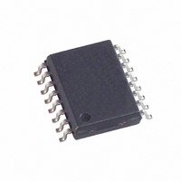
... Chapter 3: Serial Configuration Devices (EPCS1, EPCS4, EPCS16, EPCS64, and EPCS128) Data Sheet Pin Information Figure 3–22 shows the Altera serial configuration device 16-pin SOIC package and its pin-out diagram. Figure 3–22. Altera Serial Configuration Device 16-Pin SOIC Package Pin-Out Diagram Note to Figure 3– ...
Page 34
... N: Lead free. Volume 2: Configuration Handbook and Figure 3–22, the serial configuration device is an 8-pin or Pin 1 ID Altera Device Package Information Data Device EPCS1 EPCS4 EPCS16 EPCS64 EPCS128 Package Ordering Code (1) EPCS1SI8 EPCS1SI8N EPCS4SI8 EPCS4SI8N EPCS16SI16N EPCS16SI8N EPCS64SI16N EPCS128SI16N June 2011 Altera Corporation ...
Page 35
... Table 3–25. Chapter Revision History (Part Date Version June 2011 3.4 December 2009 3.3 October 2008 3.2 May 2008 3.1 June 2011 Altera Corporation Changes Made Updated Table 3–19. ■ Updated Figure 3–20. ■ Updated “Features” and “Functional Description” sections. ...
Page 36
... Updated DCLK pin information in Table 4–32. ■ Updated Figure 4–19. ■ Updated Table 4–30 and Table 4–32. ■ Updated table 4-4 to include EPCS64 support for Cyclone devices. ■ Updated tables. ■ Minor text updates. ■ Updated hot socketing AC specifications. Document Revision History June 2011 Altera Corporation ...
Page 37
... Date Version October 2003 1.2 July 2003 1.1 May 2003 1.0 June 2011 Altera Corporation Changes Made Added Serial Configuration Device Memory Access section. ■ Updated timing information in Tables 4–10 and ■ 4–11 section. Updated timing information in Tables 4-16 and 4-17. ...
Page 38
... Chapter 3: Serial Configuration Devices (EPCS1, EPCS4, EPCS16, EPCS64, and EPCS128) Data Sheet Volume 2: Configuration Handbook Document Revision History June 2011 Altera Corporation ...