EPCS16SI16N Altera, EPCS16SI16N Datasheet - Page 33
EPCS16SI16N
Manufacturer Part Number
EPCS16SI16N
Description
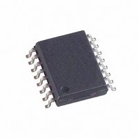
IC CONFIG DEVICE 16MBIT 16-SOIC
Manufacturer
Altera
Series
EPCSr
Specifications of EPCS16SI16N
Programmable Type
In System Programmable
Memory Size
16Mb
Voltage - Supply
3 V ~ 3.6 V
Operating Temperature
-40°C ~ 85°C
Package / Case
16-SOIC (0.300", 7.50mm Width)
Memory Type
Flash
Clock Frequency
20MHz
Supply Voltage Range
2.7V To 3.6V
Memory Case Style
SOIC
No. Of Pins
16
Operating Temperature Range
-40°C To +85°C
Rohs Compliant
Yes
Lead Free Status / RoHS Status
Lead free / RoHS Compliant
Other names
544-1240-5
EPCS16SI16
EPCS16SI16
Available stocks
Company
Part Number
Manufacturer
Quantity
Price
Company:

Part Number:
EPCS16SI16N
Manufacturer:
ALTERA
Quantity:
1 250
Company:
Part Number:
EPCS16SI16N
Manufacturer:
ALTERA44
Quantity:
540
Part Number:
EPCS16SI16N
Manufacturer:
ALTERA/阿尔特拉
Quantity:
20 000


Chapter 3: Serial Configuration Devices (EPCS1, EPCS4, EPCS16, EPCS64, and EPCS128) Data Sheet
Pin Information
Table 3–23. Serial Configuration Device Pin Description
June 2011 Altera Corporation
DATA
ASDI
nCS
DCLK
V
GND
CC
Name
Pin
2
5
1
6
3, 7, 8
4
Pin Number
Package
in 8-Pin
SOIC
Figure 3–22
pin-out diagram.
Figure 3–22. Altera Serial Configuration Device 16-Pin SOIC Package Pin-Out Diagram
Note to
(1) These pins can be left floating or connected to V
8
15
7
16
1, 2, 9
10
Pin Number
in 16-Pin
Package
Figure
SOIC
3–22:
shows the Altera serial configuration device 16-pin SOIC package and its
Output
Input
Input
Input
Power
Ground
Pin Type
The DATA output signal transfers data serially out of the serial
configuration device to the FPGA during read/configuration operation.
During read/configuration operations, the serial configuration device
is enabled by pulling nCS low. The DATA signal transitions on the
falling edge of DCLK.
The AS data input signal is used to transfer data serially into the serial
configuration device. It receives the data that should be programmed
into the serial configuration device. Data is latched on the rising edge
of DCLK.
The active low chip select input signal toggles at the beginning and
end of a valid instruction. When this signal is high, the device is
deselected and the DATA pin is tri-stated. When this signal is low, it
enables the device and puts the device in an active mode. After power
up, the serial configuration device requires a falling edge on the nCS
signal before beginning any operation.
DCLK is provided by the FPGA. This signal provides the timing of the
serial interface. The data presented on ASDI is latched to the serial
configuration device on the rising edge of DCLK. Data on the DATA pin
changes after the falling edge of DCLK and is latched into the FPGA on
the next falling edge.
Power pins connect to 3.3 V.
Ground pin.
DATA
N.C.
N.C.
N.C.
N.C.
nCS
V
V
CC
CC
CC
or EPCS128
or GND, whichever is more convenient on the board.
EPCS64,
2
3
4
5
6
7
8
EPCS16,
1
(1)
(1)
(1)
(1)
14
13
12
11
10
9
16
15
(1)
(1)
(1)
(1)
DCLK
ASDI
N.C.
N.C.
N.C.
N.C.
GND
V
CC
Description
Volume 2: Configuration Handbook
3–33
Related parts for EPCS16SI16N
Image
Part Number
Description
Manufacturer
Datasheet
Request
R

Part Number:
Description:
IC CONFIG DEVICE 1MBIT 8-SOIC
Manufacturer:
Altera
Datasheet:
Part Number:
Description:
IC CONFIG DEVICE 4MBIT 8-SOIC
Manufacturer:
Altera
Datasheet:
Part Number:
Description:
IC CONFIG DEVICE 4MBIT 8-SOIC
Manufacturer:
Altera
Datasheet:
Part Number:
Description:
IC CONFIG DEVICE 16MBIT 8-SOIC
Manufacturer:
Altera
Datasheet:

Part Number:
Description:
IC CONFIG DEVICE 64MBIT 16-SOIC
Manufacturer:
Altera
Datasheet:
Part Number:
Description:
IC CONFIG DEVICE 1MBIT 8-SOIC
Manufacturer:
Altera
Datasheet:

Part Number:
Description:
CYCLONE II STARTER KIT EP2C20N
Manufacturer:
Altera
Datasheet:


Part Number:
Description:
CPLD, EP610 Family, ECMOS Process, 300 Gates, 16 Macro Cells, 16 Reg., 16 User I/Os, 5V Supply, 35 Speed Grade, 24DIP
Manufacturer:
Altera Corporation
Datasheet:
Part Number:
Description:
CPLD, EP610 Family, ECMOS Process, 300 Gates, 16 Macro Cells, 16 Reg., 16 User I/Os, 5V Supply, 15 Speed Grade, 24DIP
Manufacturer:
Altera Corporation
Datasheet:
Part Number:
Description:
Manufacturer:
Altera Corporation
Datasheet:
Part Number:
Description:
CPLD, EP610 Family, ECMOS Process, 300 Gates, 16 Macro Cells, 16 Reg., 16 User I/Os, 5V Supply, 30 Speed Grade, 24DIP
Manufacturer:
Altera Corporation
Datasheet:
Part Number:
Description:
High-performance, low-power erasable programmable logic devices with 8 macrocells, 10ns
Manufacturer:
Altera Corporation
Datasheet: