EPCS16SI16N Altera, EPCS16SI16N Datasheet - Page 25
EPCS16SI16N
Manufacturer Part Number
EPCS16SI16N
Description
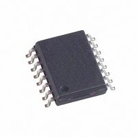
IC CONFIG DEVICE 16MBIT 16-SOIC
Manufacturer
Altera
Series
EPCSr
Specifications of EPCS16SI16N
Programmable Type
In System Programmable
Memory Size
16Mb
Voltage - Supply
3 V ~ 3.6 V
Operating Temperature
-40°C ~ 85°C
Package / Case
16-SOIC (0.300", 7.50mm Width)
Memory Type
Flash
Clock Frequency
20MHz
Supply Voltage Range
2.7V To 3.6V
Memory Case Style
SOIC
No. Of Pins
16
Operating Temperature Range
-40°C To +85°C
Rohs Compliant
Yes
Lead Free Status / RoHS Status
Lead free / RoHS Compliant
Other names
544-1240-5
EPCS16SI16
EPCS16SI16
Available stocks
Company
Part Number
Manufacturer
Quantity
Price
Company:

Part Number:
EPCS16SI16N
Manufacturer:
ALTERA
Quantity:
1 250
Company:
Part Number:
EPCS16SI16N
Manufacturer:
ALTERA44
Quantity:
540
Part Number:
EPCS16SI16N
Manufacturer:
ALTERA/阿尔特拉
Quantity:
20 000


Chapter 3: Serial Configuration Devices (EPCS1, EPCS4, EPCS16, EPCS64, and EPCS128) Data Sheet
Serial Configuration Device Memory Access
Figure 3–15. Write Bytes Operation Timing Diagram
Notes to
(1) Use the erase sector or the erase bulk instruction to initialize the memory bytes of the serial configuration devices to all 1 or 0xFF before
(2) Address bit A[23] is a don't-care bit in EPCS64. Address bits A[23..21] are don't-care bits in EPCS16. Address bits A[23..19] are don't-care
(3) For .rpd files, write the LSB of the data byte first.
June 2011 Altera Corporation
DCLK
ASDI
nCS
implementing the write bytes operation.
bits in EPCS4. Address bits A[23..17] are don't-care bits in EPCS1.
Figure
0
1
2
3–15:
Operation Code
1
3
4
5
The bytes of serial configuration devices memory must be erased to all 1 or 0xFF
before write bytes operation is implemented. This can be achieved by either using the
erase sector instruction in a sector, or the erase bulk instruction throughout the entire
memory.
Erase Bulk Operation
The erase bulk operation code is b'1100 0111, with the MSB listed first. The erase
bulk operation sets all memory bits to 1 or 0xFF. Similar to the write bytes operation,
the write enable operation must be executed prior to the erase bulk operation so that
the write enable latch bit in the status register is set to 1.
You can implement the erase bulk operation by driving nCS low and then shifting in
the erase bulk operation code on the ASDI pin. nCS must be driven high after the
eighth bit of the erase bulk operation code has been latched in.
timing diagram.
The device initiates the self-timed erase bulk cycle immediately after nCS is driven
high. Refer to t
respective EPCS devices.
You must account for this delay before accessing the memory contents. Alternatively,
you can check the write in progress bit in the status register by executing the read
status operation while the self-timed erase cycle is in progress. The write in progress
bit is 1 during the self-timed erase cycle and 0 when it is complete. The write enable
latch bit in the status register is reset to 0 before the erase cycle is complete.
Figure 3–16. Erase Bulk Operation Timing Diagram
6
7
MSB
23
8
22
9
21
10
24-Bit Address (2)
EB
3
28
in
2
29
Table 3–16
1
30
DCLK
0
ASDI
31
nCS
MSB (3)
7
32
(Note 1)
6
33
5
34
for the self-timed erase bulk cycle time for the
Data Byte 1
4
35
3
36
0
2
37
1
1
38
2
0
39
MSB (3)
Operation Code
7
40
3
6
41
4
5
42
Data Byte 2
5
4
43
44
3
6
2
45
7
1
46
0
47
Volume 2: Configuration Handbook
Figure 3–16
MSB (3)
2072 2073 2074 2075 2076 2077 2078 2079
7
6
5
Data Byte 256
4
shows the
3
2
1
0
3–25
Related parts for EPCS16SI16N
Image
Part Number
Description
Manufacturer
Datasheet
Request
R

Part Number:
Description:
IC CONFIG DEVICE 1MBIT 8-SOIC
Manufacturer:
Altera
Datasheet:
Part Number:
Description:
IC CONFIG DEVICE 4MBIT 8-SOIC
Manufacturer:
Altera
Datasheet:
Part Number:
Description:
IC CONFIG DEVICE 4MBIT 8-SOIC
Manufacturer:
Altera
Datasheet:
Part Number:
Description:
IC CONFIG DEVICE 16MBIT 8-SOIC
Manufacturer:
Altera
Datasheet:

Part Number:
Description:
IC CONFIG DEVICE 64MBIT 16-SOIC
Manufacturer:
Altera
Datasheet:
Part Number:
Description:
IC CONFIG DEVICE 1MBIT 8-SOIC
Manufacturer:
Altera
Datasheet:

Part Number:
Description:
CYCLONE II STARTER KIT EP2C20N
Manufacturer:
Altera
Datasheet:


Part Number:
Description:
CPLD, EP610 Family, ECMOS Process, 300 Gates, 16 Macro Cells, 16 Reg., 16 User I/Os, 5V Supply, 35 Speed Grade, 24DIP
Manufacturer:
Altera Corporation
Datasheet:
Part Number:
Description:
CPLD, EP610 Family, ECMOS Process, 300 Gates, 16 Macro Cells, 16 Reg., 16 User I/Os, 5V Supply, 15 Speed Grade, 24DIP
Manufacturer:
Altera Corporation
Datasheet:
Part Number:
Description:
Manufacturer:
Altera Corporation
Datasheet:
Part Number:
Description:
CPLD, EP610 Family, ECMOS Process, 300 Gates, 16 Macro Cells, 16 Reg., 16 User I/Os, 5V Supply, 30 Speed Grade, 24DIP
Manufacturer:
Altera Corporation
Datasheet:
Part Number:
Description:
High-performance, low-power erasable programmable logic devices with 8 macrocells, 10ns
Manufacturer:
Altera Corporation
Datasheet: