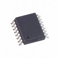
EPCS16SI16N Altera, EPCS16SI16N Datasheet - Page 29

EPCS16SI16N
Manufacturer Part Number
EPCS16SI16N
Description
IC CONFIG DEVICE 16MBIT 16-SOIC
Manufacturer
Altera
Series
EPCSr
Specifications of EPCS16SI16N
Programmable Type
In System Programmable
Memory Size
16Mb
Voltage - Supply
3 V ~ 3.6 V
Operating Temperature
-40°C ~ 85°C
Package / Case
16-SOIC (0.300", 7.50mm Width)
Memory Type
Flash
Clock Frequency
20MHz
Supply Voltage Range
2.7V To 3.6V
Memory Case Style
SOIC
No. Of Pins
16
Operating Temperature Range
-40°C To +85°C
Rohs Compliant
Yes
Lead Free Status / RoHS Status
Lead free / RoHS Compliant
Other names
544-1240-5
EPCS16SI16
EPCS16SI16
Available stocks
Company
Part Number
Manufacturer
Quantity
Price
Company:
Part Number:
EPCS16SI16N
Manufacturer:
ALTERA
Quantity:
1 250
Company:
Part Number:
EPCS16SI16N
Manufacturer:
ALTERA44
Quantity:
540
Part Number:
EPCS16SI16N
Manufacturer:
ALTERA/阿尔特拉
Quantity:
20 000
Chapter 3: Serial Configuration Devices (EPCS1, EPCS4, EPCS16, EPCS64, and EPCS128) Data Sheet
Timing Information
Figure 3–20. AS Configuration Timing
Note to
(1) t
June 2011 Altera Corporation
CONF_DONE
INIT_DONE
User I/O
nCONFIG
nSTATUS
DATA0
CD2UM
nCSO
DCLK
ASDO
Figure
is a FPGA dependent parameter. For more information, refer to the respective device configuration chapters.
Tri-stated with internal pull-up resistor
t
3–20:
CF2ST1
f
f
1
Existing batches of EPCS1 and EPCS4 manufactured on 0.15 µm process geometry
support AS configuration up to 40 MHz. However, batches of EPCS1 and EPCS4
manufactured on 0.18 µm process geometry support only up to 20 MHz. EPCS16,
EPCS64, and EPCS128 are not affected.
For information about product traceability and transition date to differentiate
between 0.15 µm process geometry and 0.18 µm process geometry EPCS1 and EPCS4,
refer to the Process Change Notification
Family.
Figure 3–20
serial configuration device.
For more information about the timing parameters in
respective FPGA family handbook Configuration chapter.
Read Address
shows the timing waveform for FPGA AS configuration scheme using a
bit N
bit N-1
bit 1
PCN 0514: Manufacturing Changes on EPCS
bit 0
Figure
t
Volume 2: Configuration Handbook
CD2UM
3–20, refer to the
(1)
User Mode
3–29


