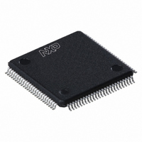
PCF2113DH/4,557 NXP Semiconductors, PCF2113DH/4,557 Datasheet - Page 11

PCF2113DH/4,557
Manufacturer Part Number
PCF2113DH/4,557
Description
IC LCD CONTROLLER/DRIVER 100LQFP
Manufacturer
NXP Semiconductors
Datasheet
1.PCF2113DH4557.pdf
(65 pages)
Specifications of PCF2113DH/4,557
Package / Case
100-LQFP
Display Type
LCD
Configuration
5 X 8 (Matrix)
Interface
I²C
Voltage - Supply
2.2 V ~ 4 V
Operating Temperature
-40°C ~ 85°C
Mounting Type
Surface Mount
Number Of Digits
40
Maximum Clock Frequency
450 KHz
Operating Supply Voltage
1.8 V to 5.5 V
Maximum Power Dissipation
400 mW
Maximum Operating Temperature
+ 75 C
Attached Touch Screen
No
Maximum Supply Current
50 mA
Minimum Operating Temperature
- 20 C
Operating Supply Voltage (typ)
2.5/3.3/5V
Package Type
LQFP
Pin Count
100
Mounting
Surface Mount
Power Dissipation
400mW
Operating Supply Voltage (min)
1.8V
Operating Supply Voltage (max)
5.5V
Lead Free Status / RoHS Status
Lead free / RoHS Compliant
Current - Supply
-
Digits Or Characters
-
Lead Free Status / Rohs Status
Lead free / RoHS Compliant
Other names
935276328557
PCF2113DH/4
PCF2113DH/4
PCF2113DH/4
PCF2113DH/4
Available stocks
Company
Part Number
Manufacturer
Quantity
Price
Company:
Part Number:
PCF2113DH/4,557
Manufacturer:
NXP Semiconductors
Quantity:
10 000
NXP Semiconductors
PCF2113_FAM_4
Product data sheet
8.3 Oscillator
8.4 External clock
8.5 Power-on reset
8.6 Registers
8.7 Busy flag
Table 6.
[1]
The on-chip oscillator provides the clock signal for the display system. No external
components are required and the OSC pin must be connected to V
If an external clock is to be used, this input is at the OSC pin. The resulting display frame
frequency is given by:
Only in the Power-down mode is the clock allowed to be stopped (pin OSC connected to
V
The on-chip power-on reset block initializes the chip after power-on or power failure. This
is a synchronous reset and requires 3 oscillator cycles to be executed.
The PCF2113x has two 8-bit registers: an Instruction Register (IR) and a Data
Register (DR). The Register Select (RS) signal determines which register will be
accessed. The instruction register stores instruction codes such as ‘display clear’, ‘cursor
shift’, and address information for the Display Data RAM (DDRAM) and Character
Generator RAM (CGRAM). The instruction register can be written to but not read from by
the system controller.
The data register temporarily stores data to be read from the DDRAM and CGRAM. When
reading, data from the DDRAM or CGRAM corresponding to the address in the instruction
register is written to the data register prior to being read by the ‘read data’ instruction.
The busy flag indicates the internal status of the PCF2113x. A logic 1 indicates that the
chip is busy and further instructions will not be accepted. The busy flag is output to
pin DB7 when bit RS = 0 and bit R/W = 1. Instructions must only be written after checking
that the busy flag is at logic 0 or waiting for the required number of cycles.
Multiplex
rate
1:18
1:9
1:2
SS
), otherwise the LCD is frozen in a DC state.
The values in the table are given relative to V
Bias levels as a function of multiplex rate
Number
of levels
5
5
4
f
Bias voltages
V
V
V
V
Rev. 04 — 4 March 2008
fr LCD
1
LCD
LCD
LCD
=
----------- -
3072
V
3
3
2
f
4
4
3
osc
2
[1]
LCD
V
V
1
1
2
SS
2
2
3
3
, e.g.
3
4
means {
V
1
1
1
2
2
3
4
3
4
LCD controllers/drivers
(V
LCD
DD1
V
1
1
1
PCF2113x
4
4
3
5
.
© NXP B.V. 2008. All rights reserved.
V
SS
)} + V
V
V
V
V
SS
6
SS
SS
SS
.
11 of 65


