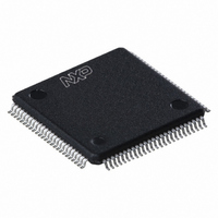
PCF2113DH/4,557 NXP Semiconductors, PCF2113DH/4,557 Datasheet - Page 36

PCF2113DH/4,557
Manufacturer Part Number
PCF2113DH/4,557
Description
IC LCD CONTROLLER/DRIVER 100LQFP
Manufacturer
NXP Semiconductors
Datasheet
1.PCF2113DH4557.pdf
(65 pages)
Specifications of PCF2113DH/4,557
Package / Case
100-LQFP
Display Type
LCD
Configuration
5 X 8 (Matrix)
Interface
I²C
Voltage - Supply
2.2 V ~ 4 V
Operating Temperature
-40°C ~ 85°C
Mounting Type
Surface Mount
Number Of Digits
40
Maximum Clock Frequency
450 KHz
Operating Supply Voltage
1.8 V to 5.5 V
Maximum Power Dissipation
400 mW
Maximum Operating Temperature
+ 75 C
Attached Touch Screen
No
Maximum Supply Current
50 mA
Minimum Operating Temperature
- 20 C
Operating Supply Voltage (typ)
2.5/3.3/5V
Package Type
LQFP
Pin Count
100
Mounting
Surface Mount
Power Dissipation
400mW
Operating Supply Voltage (min)
1.8V
Operating Supply Voltage (max)
5.5V
Lead Free Status / RoHS Status
Lead free / RoHS Compliant
Current - Supply
-
Digits Or Characters
-
Lead Free Status / Rohs Status
Lead free / RoHS Compliant
Other names
935276328557
PCF2113DH/4
PCF2113DH/4
PCF2113DH/4
PCF2113DH/4
Available stocks
Company
Part Number
Manufacturer
Quantity
Price
Company:
Part Number:
PCF2113DH/4,557
Manufacturer:
NXP Semiconductors
Quantity:
10 000
NXP Semiconductors
11. Interfaces to microcontroller
PCF2113_FAM_4
Product data sheet
11.1 Parallel interface
The PCF2113x can send data in either two 4-bit operations or one 8-bit operation and can
thus interface to 4-bit or 8-bit microcontrollers.
In 8-bit mode data is transferred as 8-bit bytes using the 8 data lines DB7 to DB0. Three
further control lines E, RS and R/W are required (see
In 4-bit mode data is transferred in two cycles of 4 bits each using pins DB7 to DB4 for the
transaction. The higher order bits (corresponding to bits DB7 to DB4 in 8-bit mode) are
sent in the first cycle and the lower order bits (corresponding to bits DB3 to DB0 in 8-bit
mode) in the second cycle. Data transfer is complete after two 4-bit data transfers. It
should be noted that two cycles are also required for the busy flag check. 4-bit operation is
selected by instruction: see
protocol.
In 4-bit mode, pins DB3 to DB0 must be left open-circuit. They are pulled up to V
internally.
Fig 22. 4-bit transfer example
R/W
DB7
DB6
DB5
DB4
RS
E
instruction
IR7
IR6
IR5
IR4
write
Rev. 04 — 4 March 2008
IR3
IR2
IR1
IR0
Figure
22,
AC6
AC5
AC4
BF
Figure 23
address counter read
busy flag and
and
AC3
AC2
AC1
AC0
Figure 24
Section
7).
for examples of bus
DR7
DR6
DR5
DR4
LCD controllers/drivers
data register
PCF2113x
read
© NXP B.V. 2008. All rights reserved.
DR3
DR2
DR1
DR0
mga804
DD
36 of 65


