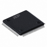
PCF2113DH/4,557 NXP Semiconductors, PCF2113DH/4,557 Datasheet - Page 30

PCF2113DH/4,557
Manufacturer Part Number
PCF2113DH/4,557
Description
IC LCD CONTROLLER/DRIVER 100LQFP
Manufacturer
NXP Semiconductors
Datasheet
1.PCF2113DH4557.pdf
(65 pages)
Specifications of PCF2113DH/4,557
Package / Case
100-LQFP
Display Type
LCD
Configuration
5 X 8 (Matrix)
Interface
I²C
Voltage - Supply
2.2 V ~ 4 V
Operating Temperature
-40°C ~ 85°C
Mounting Type
Surface Mount
Number Of Digits
40
Maximum Clock Frequency
450 KHz
Operating Supply Voltage
1.8 V to 5.5 V
Maximum Power Dissipation
400 mW
Maximum Operating Temperature
+ 75 C
Attached Touch Screen
No
Maximum Supply Current
50 mA
Minimum Operating Temperature
- 20 C
Operating Supply Voltage (typ)
2.5/3.3/5V
Package Type
LQFP
Pin Count
100
Mounting
Surface Mount
Power Dissipation
400mW
Operating Supply Voltage (min)
1.8V
Operating Supply Voltage (max)
5.5V
Lead Free Status / RoHS Status
Lead free / RoHS Compliant
Current - Supply
-
Digits Or Characters
-
Lead Free Status / Rohs Status
Lead free / RoHS Compliant
Other names
935276328557
PCF2113DH/4
PCF2113DH/4
PCF2113DH/4
PCF2113DH/4
Available stocks
Company
Part Number
Manufacturer
Quantity
Price
Company:
Part Number:
PCF2113DH/4,557
Manufacturer:
NXP Semiconductors
Quantity:
10 000
NXP Semiconductors
PCF2113_FAM_4
Product data sheet
9.10 Write data to CGRAM or DDRAM
9.11 Read data from CGRAM or DDRAM
9.8 Set DDRAM address
9.9 Read busy flag and read address
Remark: the CGRAM address uses the same address register as the DDRAM address
and consists of 7 bits (A6h to A0h). With the ‘set CGRAM address’ command, only
bits DB5 to DB0 are set. Bit DB6 can be set using the ‘set DDRAM address’ command
first, or by using the auto-increment feature during CGRAM write. All bits DB6 to DB0 can
be read using the ‘read busy flag’ and ‘read address’ command.
When writing to the lower part of the CGRAM, ensure that bit DB6 of the address is not
set (e.g. by an earlier DDRAM write or read action).
‘Set DDRAM address’ writes the DDRAM address ADD into the address counter
(A6h to A0h). Data can then be written to or read from the DDRAM.
‘Read busy flag and address counter’ reads the Busy Flag (BF) and Address
Counter (AC). BF = 1 indicates that an internal operation is in progress. The next
instruction will not be executed until BF = 0. It is recommended that the BF status is
checked before the next write operation is executed.
At the same time, the value of the address counter (A6h to A0h) is read out, into DB6 to
DB0. The address counter is used by both CGRAM and DDRAM, and its value is
determined by the previous instruction.
‘Write data’ writes binary 8-bit data DB7 to DB0 to the CGRAM or the DDRAM.
Whether the CGRAM or DDRAM is to be written into is determined by the previous ‘set
CGRAM address’ or ‘set DDRAM address’ command. After writing, the address
automatically increments or decrements by 1, in accordance with the entry mode. Only
bits DB4 to DB0 of CGRAM data are valid, bits DB7 to DB5 are ‘not relevant’.
‘Read data’ reads binary 8-bit data DB7 to DB0 from the CGRAM or DDRAM.
The most recent ‘set address’ command determines whether the CGRAM or DDRAM is to
be read.
The ‘read data’ instruction gates the content of the Data Register (DR) to the bus while
pin E is HIGH. After pin E goes LOW again, internal operation increments (or decrements)
the AC and stores RAM data corresponding to the new AC into the DR.
There are only three instructions that update the DR:
Other instructions (e.g. ‘write data’, ‘cursor/display shift’, ‘clear display’ and ‘return home’)
do not modify the data register content.
•
•
•
‘Set CGRAM address’
‘Set DDRAM address’
‘Read data’ from CGRAM or DDRAM
Rev. 04 — 4 March 2008
LCD controllers/drivers
PCF2113x
© NXP B.V. 2008. All rights reserved.
30 of 65


