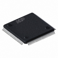
PCF2113DH/4,557 NXP Semiconductors, PCF2113DH/4,557 Datasheet - Page 54

PCF2113DH/4,557
Manufacturer Part Number
PCF2113DH/4,557
Description
IC LCD CONTROLLER/DRIVER 100LQFP
Manufacturer
NXP Semiconductors
Datasheet
1.PCF2113DH4557.pdf
(65 pages)
Specifications of PCF2113DH/4,557
Package / Case
100-LQFP
Display Type
LCD
Configuration
5 X 8 (Matrix)
Interface
I²C
Voltage - Supply
2.2 V ~ 4 V
Operating Temperature
-40°C ~ 85°C
Mounting Type
Surface Mount
Number Of Digits
40
Maximum Clock Frequency
450 KHz
Operating Supply Voltage
1.8 V to 5.5 V
Maximum Power Dissipation
400 mW
Maximum Operating Temperature
+ 75 C
Attached Touch Screen
No
Maximum Supply Current
50 mA
Minimum Operating Temperature
- 20 C
Operating Supply Voltage (typ)
2.5/3.3/5V
Package Type
LQFP
Pin Count
100
Mounting
Surface Mount
Power Dissipation
400mW
Operating Supply Voltage (min)
1.8V
Operating Supply Voltage (max)
5.5V
Lead Free Status / RoHS Status
Lead free / RoHS Compliant
Current - Supply
-
Digits Or Characters
-
Lead Free Status / Rohs Status
Lead free / RoHS Compliant
Other names
935276328557
PCF2113DH/4
PCF2113DH/4
PCF2113DH/4
PCF2113DH/4
Available stocks
Company
Part Number
Manufacturer
Quantity
Price
Company:
Part Number:
PCF2113DH/4,557
Manufacturer:
NXP Semiconductors
Quantity:
10 000
NXP Semiconductors
Table 25.
PCF2113_FAM_4
Product data sheet
Step
7
8
9
10
11
12 to 15
16
17
18
19
20
21
22
I
I
slave address for write
SA6 SA5 SA4 SA3 SA2 SA1 SA0 R/W Ack
0
send a control byte for ‘write data’
Co
0
‘write data’ to DDRAM
DB7 DB6 DB5 DB4 DB3 DB2 DB1 DB0 Ack
0
‘write data’ to DDRAM
DB7 DB6 DB5 DB4 DB3 DB2 DB1 DB0 Ack
0
‘write data’ to DDRAM
DB7 DB6 DB5 DB4 DB3 DB2 DB1 DB0 Ack
0
(optional I
write (as step 8)
control byte
Co
1
return home
DB7 DB6 DB5 DB4 DB3 DB2 DB1 DB0 Ack
0
I
slave address for read
SA6 SA5 SA4 SA3 SA2 SA1 SA0 R/W Ack
0
control byte for read
Co
0
2
2
2
Example of I
C-bus byte
C-bus start
C-bus start
1
RS
1
1
1
1
RS
0
0
1
RS
1
2
C-bus stop) I
1
0
0
0
0
0
0
0
0
1
0
1
2
C-bus operation; 1-line display (using internal reset, assuming SA0 = V
0
0
0
1
0
1
0
1
0
0
1
0
2
C-bus start + slave address for
0
0
0
0
0
0
1
0
0
0
0
0
0
:
0
0
1
0
0
0
:
0
0
0
1
0
0
0
0
0
0
0
0
1
0
1
0
0
Rev. 04 — 4 March 2008
0
0
0
0
0
0
0
1
0
0
1
0
Ack
Ack
Ack
1
1
1
1
1
1
1
1
1
Display
P
PH
PHILIPS
PHILIPS
PHILIPS
PHILIPS
PHILIPS
PHILIPS
PHILIPS
Operation
to write data to DDRAM, RS must be
set to 1 so a control byte is needed
writes ‘P’; the DDRAM is selected at
power-up; the cursor is incremented
by 1 and shifted to the right
writes ‘H’
writes ‘ILIP’
writes ‘S’
sets DDRAM address 0 in address
counter (also returns shifted display
to original position; DDRAM contents
unchanged); this instruction does not
update the Data Register (DR)
during the acknowledge cycle the
content of DR is loaded into the
internal I
out; in the previous instruction neither
a ‘set address’ nor a ‘read data’ has
been performed, so the content of the
DR was unknown; the R/W has to be
set to 1 while still in the I
mode
DDRAM content is read from the
following instructions
2
C-bus interface to be shifted
LCD controllers/drivers
PCF2113x
SS
© NXP B.V. 2008. All rights reserved.
)
[1]
…continued
2
C-bus write
54 of 65


