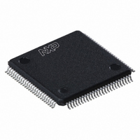
PCF2113DH/4,557 NXP Semiconductors, PCF2113DH/4,557 Datasheet - Page 9

PCF2113DH/4,557
Manufacturer Part Number
PCF2113DH/4,557
Description
IC LCD CONTROLLER/DRIVER 100LQFP
Manufacturer
NXP Semiconductors
Datasheet
1.PCF2113DH4557.pdf
(65 pages)
Specifications of PCF2113DH/4,557
Package / Case
100-LQFP
Display Type
LCD
Configuration
5 X 8 (Matrix)
Interface
I²C
Voltage - Supply
2.2 V ~ 4 V
Operating Temperature
-40°C ~ 85°C
Mounting Type
Surface Mount
Number Of Digits
40
Maximum Clock Frequency
450 KHz
Operating Supply Voltage
1.8 V to 5.5 V
Maximum Power Dissipation
400 mW
Maximum Operating Temperature
+ 75 C
Attached Touch Screen
No
Maximum Supply Current
50 mA
Minimum Operating Temperature
- 20 C
Operating Supply Voltage (typ)
2.5/3.3/5V
Package Type
LQFP
Pin Count
100
Mounting
Surface Mount
Power Dissipation
400mW
Operating Supply Voltage (min)
1.8V
Operating Supply Voltage (max)
5.5V
Lead Free Status / RoHS Status
Lead free / RoHS Compliant
Current - Supply
-
Digits Or Characters
-
Lead Free Status / Rohs Status
Lead free / RoHS Compliant
Other names
935276328557
PCF2113DH/4
PCF2113DH/4
PCF2113DH/4
PCF2113DH/4
Available stocks
Company
Part Number
Manufacturer
Quantity
Price
Company:
Part Number:
PCF2113DH/4,557
Manufacturer:
NXP Semiconductors
Quantity:
10 000
NXP Semiconductors
Table 5.
All x/y coordinates represent the position of the center of each pad with respect to the center (x/y = 0) of the chip (see
Figure
[1]
[2]
[3]
[4]
[5]
[6]
PCF2113_FAM_4
Product data sheet
Symbol
C1
R8
R7
R6
R5
R4
R3
R2
R1
R17
SCL
SDA
E
RS
R/W
DB7
DB6
DB5
DB4
DB3/SA0
DB2
DB1
DB0
V
V
dummy pad 7
dummy pad 8
DD2
DD3
When the on-chip oscillator is used this pad must be connected to V
When V
supplied, this should be done via V
In the LQFP100 version this signal is connected internally and is not accessible.
When the I
V
When the parallel bus is used, the pins SCL and SDA must be connected to pin V
When the 4-bit interface is used without reading out from the PCF2113x (bit R/W is set permanently to logic 0), the unused ports DB0 to
DB3 can either be connected to V
DB7 may be used as the busy flag, signalling that internal operations are not yet completed. In 4-bit operations the four higher order
lines DB7 to DB4 are used; DB3 to DB0 must be left open-circuit except for I
V
DD1
DD2
3).
or left open-circuit.
and V
LCD
Pin and bonding pad description
2
DD3
C-bus is used, the parallel interface pin E must be LOW. In the I
is generated internally, pins V
Pin
77
78
79
80
81
82
83
84
85
86
87
88
89
90
91
92
93
94
95
96
97
98
99
100
-
-
-
must always be equal.
Type
O
O
O
O
O
O
O
O
O
O
I
I/O
I
I
I
I/O
I/O
I/O
I/O
I/O
I/O
I/O
I/O
P
P
-
-
SS1
LCDIN
or V
Pad
86
87
88
89
90
91
92
93
94
95
96
97
98
99
100
101
102
103
104
105
106
107
108
109
110
111
112
. In this case only pins V
LCDIN
DD1
instead of leaving them open-circuit.
, V
…continued
X ( m)
LCDOUT
1630
1630
1630
1630
1630
1630
1630
1630
1630
1630
1630
1630
1630
1630
1630
1630
1630
1630
1630
1630
1630
1630
1630
1630
1630
1630
1465
Rev. 04 — 4 March 2008
and V
LCDSENSE
Y ( m)
1185
1115
1045
975
905
835
765
695
625
555
375
305
85
LCDOUT
15
115
215
315
415
515
615
715
815
915
1015
1235
1395
1550
DD1
.
and V
must be connected together. When an external V
2
2
C-bus read mode pins DB7 to DB0 must be connected to
C-bus operations (see
Description
LCD column driver output
LCD row driver output
LCD row driver output
LCD row driver output
LCD row driver output
LCD row driver output
LCD row driver output
LCD row driver output
LCD row driver output
LCD row driver output
I
I
data bus clock input
register select input
read or write input
8-bit bidirectional bus bit 7
8-bit bidirectional bus bit 6
8-bit bidirectional bus bit 5
8-bit bidirectional bus bit 4
8-bit bidirectional bus bit 3 or I
address input
8-bit bidirectional bus bit 2
8-bit bidirectional bus bit 1
8-bit bidirectional bus bit 0
supply voltage 2 for V
supply voltage 3 for V
-
-
LCDSENSE
2
2
C-bus serial clock input
C-bus serial data input/output
SS1
or pin V
must be connected together.
DD1
; they must not be left open-circuit.
Table note
LCD
LCD
LCD controllers/drivers
generator
generator
PCF2113x
4).
2
© NXP B.V. 2008. All rights reserved.
C-bus
LCD
is
9 of 65
[4]
[4]
[4]
[5]
[4][5]
[6]
[3][6]


