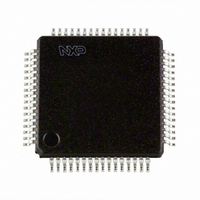
PCF8578H/1,118 NXP Semiconductors, PCF8578H/1,118 Datasheet - Page 17

PCF8578H/1,118
Manufacturer Part Number
PCF8578H/1,118
Description
IC LCD DRIVER DOT MATRIX 64-LQFP
Manufacturer
NXP Semiconductors
Datasheet
1.PCF8578H1118.pdf
(46 pages)
Specifications of PCF8578H/1,118
Display Type
LCD
Configuration
Dot Matrix
Interface
I²C
Voltage - Supply
2.5 V ~ 6 V
Operating Temperature
-40°C ~ 85°C
Mounting Type
Surface Mount
Package / Case
64-LQFP
Lead Free Status / RoHS Status
Lead free / RoHS Compliant
Current - Supply
-
Digits Or Characters
-
Lead Free Status / Rohs Status
Details
Other names
935276284118
PCF8578H/1-T
PCF8578H/1-T
PCF8578H/1-T
PCF8578H/1-T
Available stocks
Company
Part Number
Manufacturer
Quantity
Price
Company:
Part Number:
PCF8578H/1,118
Manufacturer:
NXP Semiconductors
Quantity:
10 000
NXP Semiconductors
PCF8578_6
Product data sheet
8.8.1 Bit transfer
8.8.2 START and STOP conditions
8.8.3 System configuration
8.7 Row and column drivers
8.8 Characteristics of the I
Outputs R0 to R7 and C32 to C39 are fixed as row and column drivers respectively. The
remaining 24 outputs R8/C8 to R31/C31 are programmable and may be configured (in
blocks of 8) to be either row or column drivers. The row select signal is produced
sequentially at each output from R0 up to the number defined by the multiplex rate (see
Table
programmable outputs (R8/C8 to R31/C31) are defined as row drivers and the outputs
C32 to C39 should be left open-circuit.
Using a 1:16 multiplex rate, two sets of row outputs are driven, thus facilitating split-screen
configurations, i.e. a row select pulse appears simultaneously at R0 and R16/C16, R1 and
R17/C17 etc. Similarly, using a multiplex rate of 1:8, four sets of row outputs are driven
simultaneously. Driver outputs must be connected directly to the LCD. Unused outputs
should be left open circuit.
Depending on the multiplex rate the following outputs are rows:
The configuration of the outputs (row or column) and the selection of the appropriate
driver waveforms are controlled by the display mode controller.
The I
The two lines are a Serial Data Line (SDA) and a Serial Clock Line (SCL) which must be
connected to a positive supply via a pull-up resistor. Data transfer may be initiated only
when the bus is not busy.
One data bit is transferred during each clock pulse. The data on the SDA line must remain
stable during the HIGH period of the clock pulse as changes in the data line at this
moment will be interpreted as control signals.
Both data and clock lines remain HIGH when the bus is not busy. A HIGH-to-LOW
transition of the data line, while the clock is HIGH, is defined as the START condition (S).
A LOW-to-HIGH transition of the data line while the clock is HIGH, is defined as the STOP
condition (P).
A device transmitting a message is a transmitter, a device receiving a message is the
receiver. The device that controls the message flow is the master and the devices which
are controlled by the master are the slaves.
•
•
•
•
In MUX 1:8 R0 to R7
In MUX 1:16 R0 to R15/C15
In MUX 1:24 R0 to R23/C23
In MUX 1:32 R0 to R31/C31
2
4). In mixed mode the remaining outputs are configured as columns. In row mode all
C-bus is for bidirectional, two-line communication between different ICs or modules.
Rev. 06 — 5 May 2009
2
C-bus
LCD row/column driver for dot matrix graphic displays
PCF8578
© NXP B.V. 2009. All rights reserved.
17 of 46


