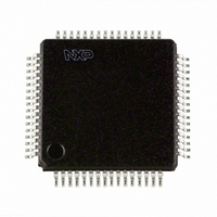
PCF8578H/1,118 NXP Semiconductors, PCF8578H/1,118 Datasheet - Page 21

PCF8578H/1,118
Manufacturer Part Number
PCF8578H/1,118
Description
IC LCD DRIVER DOT MATRIX 64-LQFP
Manufacturer
NXP Semiconductors
Datasheet
1.PCF8578H1118.pdf
(46 pages)
Specifications of PCF8578H/1,118
Display Type
LCD
Configuration
Dot Matrix
Interface
I²C
Voltage - Supply
2.5 V ~ 6 V
Operating Temperature
-40°C ~ 85°C
Mounting Type
Surface Mount
Package / Case
64-LQFP
Lead Free Status / RoHS Status
Lead free / RoHS Compliant
Current - Supply
-
Digits Or Characters
-
Lead Free Status / Rohs Status
Details
Other names
935276284118
PCF8578H/1-T
PCF8578H/1-T
PCF8578H/1-T
PCF8578H/1-T
Available stocks
Company
Part Number
Manufacturer
Quantity
Price
Company:
Part Number:
PCF8578H/1,118
Manufacturer:
NXP Semiconductors
Quantity:
10 000
NXP Semiconductors
PCF8578_6
Product data sheet
8.9.1 Data pointer
8.9.2 Subaddress counter
8.10 Command decoder
8.9 Display RAM
master receiver must signal an end of data to the slave transmitter, by not generating an
acknowledge on the last byte clocked out of the slave. The slave transmitter then leaves
the data line HIGH, enabling the master to generate a STOP condition (P).
Display bytes are written into, or read from the RAM at the address specified by the data
pointer and subaddress counter. Both the data pointer and subaddress counter are
automatically incremented, enabling a stream of data to be transferred either to, or from
the intended devices.
In multiple device applications, the hardware subaddress pins of the PCF8579s (A0 to A3)
are connected to V
more devices share the same slave address, then each device must be allocated to a
unique hardware subaddress.
The PCF8578 contains a 32
is divided into 4 banks of 40 bytes (4
transferred to and from the RAM via the I
cannot be displayed but are available for general data storage and provide compatibility
with the PCF8579. There is a direct correspondence between X-address and column
output number.
The addressing mechanism for the display RAM is realized using the data pointer. This
allows an individual data byte or a series of data bytes to be written into, or read from, the
display RAM, controlled by commands sent on the I
The storage and retrieval of display data is dependent on the content of the subaddress
counter. Storage takes place only when the contents of the subaddress counter match
with the hardware subaddress. The hardware subaddress of the PCF8578, valid in mixed
mode only, is fixed at 0000.
The command decoder identifies command bytes that arrive on the I
The five commands available to the PCF8578 are defined in
Table 9.
The most-significant bit of a command is the continuation bit C (see
Figure
Command
Bit
set-mode
set-start-bank
device-select
RAM-access
load-X-address
16). Commands are transferred in WRITE mode only.
Definition of PCF8578 commands
SS
Operation code
7
C
C
C
C
C
or V
Rev. 06 — 5 May 2009
DD
6
1
1
1
1
0
to represent the desired hardware subaddress code. If two or
40-bit static RAM which stores the display data. The RAM
LCD row/column driver for dot matrix graphic displays
5
0
1
1
1
X[5:0]
8
4
T
1
0
1
2
C-bus. The first eight columns of data (0 to 7)
40 bits). During RAM access, data is
3
E[1:0]
1
A[3:0]
G[1:0]
2
C-bus.
2
1
Table
1
M[1:0]
B[1:0]
Y[1:0]
9.
2
Table 10
C-bus.
0
PCF8578
© NXP B.V. 2009. All rights reserved.
Reference
Table 11
Table 12
Table 13
Table 14
Table 15
and
21 of 46


