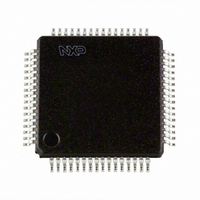
PCF8578H/1,118 NXP Semiconductors, PCF8578H/1,118 Datasheet - Page 19

PCF8578H/1,118
Manufacturer Part Number
PCF8578H/1,118
Description
IC LCD DRIVER DOT MATRIX 64-LQFP
Manufacturer
NXP Semiconductors
Datasheet
1.PCF8578H1118.pdf
(46 pages)
Specifications of PCF8578H/1,118
Display Type
LCD
Configuration
Dot Matrix
Interface
I²C
Voltage - Supply
2.5 V ~ 6 V
Operating Temperature
-40°C ~ 85°C
Mounting Type
Surface Mount
Package / Case
64-LQFP
Lead Free Status / RoHS Status
Lead free / RoHS Compliant
Current - Supply
-
Digits Or Characters
-
Lead Free Status / Rohs Status
Details
Other names
935276284118
PCF8578H/1-T
PCF8578H/1-T
PCF8578H/1-T
PCF8578H/1-T
Available stocks
Company
Part Number
Manufacturer
Quantity
Price
Company:
Part Number:
PCF8578H/1,118
Manufacturer:
NXP Semiconductors
Quantity:
10 000
NXP Semiconductors
PCF8578_6
Product data sheet
8.8.5 I
8.8.6 Input filters
8.8.7 I
The I
data bytes. It performs the conversion of the data input (serial-to-parallel) and the data
output (parallel-to-serial). The PCF8578 acts as an I
mixed mode, and as a slave receiver in row mode. A slave device cannot control bus
communication.
To enhance noise immunity in electrically adverse environments, RC low-pass filters are
provided on the SDA and SCL lines.
Two 7-bit slave addresses (0111 100 and 0111 101) are reserved for both the PCF8578
and PCF8579. The least significant bit of the slave address is set by connecting input SA0
to either logic 0 (V
be distinguished on the same I
In most applications the PCF8578 will have the same slave address as the PCF8579.
The I
condition (S) from the I
read/write bit. All devices with this slave address acknowledge in parallel. All other devices
ignore the bus transfer.
In WRITE mode (indicated by setting the read/write bit LOW) one or more commands
follow the slave address acknowledgement. The commands are also acknowledged by all
addressed devices on the bus. The last command must clear the continuation bit C.
After the last command a series of data bytes may follow. The acknowledgement after
each byte is made only by the (A0, A1, A2 and A3) addressed PCF8579 or PCF8578 with
its implicit subaddress 0. After the last data byte has been acknowledged, the I
master issues a STOP condition (P).
2
2
1. One PCF8578 to operate with up to 32 PCF8579s on the same I
2. The use of two types of LCD multiplex schemes on the same I
Fig 14. Acknowledgement on the I
C-bus controller
C-bus protocol
applications.
2
2
C-bus controller detects the I
C-bus protocol is shown in
BY TRANSMITTER
DATA OUTPUT
DATA OUTPUT
The general characteristics and detailed specification of the I
BY RECEIVER
SCL FROM
MASTER
SS
) or logic 1 (V
condition
START
2
S
C-bus master, which is followed by the desired slave address and
Rev. 06 — 5 May 2009
2
LCD row/column driver for dot matrix graphic displays
C-bus which allows:
Figure
DD
2
1
2
C-bus protocol, slave address, commands and display
C-bus
). Therefore, two types of PCF8578 or PCF8579 can
15. All communications are initiated with a START
2
2
C-bus slave transmitter/receiver in
2
C-bus are available on request.
8
2
C-bus.
2
C-bus for very large
acknowledgement
PCF8578
© NXP B.V. 2009. All rights reserved.
clock pulse for
9
mba606
2
C-bus
19 of 46


