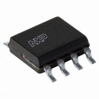
PCA9512AD,112 NXP Semiconductors, PCA9512AD,112 Datasheet

PCA9512AD,112
Specifications of PCA9512AD,112
935279721112
PCA9512AD
Related parts for PCA9512AD,112
PCA9512AD,112 Summary of contents
Page 1
PCA9512A Level shifting hot swappable I Rev. 01 — 7 October 2005 1. General description The PCA9512A is a hot swappable I insertion into a live backplane without corruption of the data and clock buses and includes two dedicated supply ...
Page 2
Philips Semiconductors ESD protection exceeds 2000 V HBM per JESD22-A114, 200 V MM per JESD22-A115, and 1000 V CDM per JESD22-C101 Latch-up testing is done to JEDEC Standard JESD78 which exceeds 100 mA Packages offered: SO8, TSSOP8 (MSOP8) 3. Applications ...
Page 3
Philips Semiconductors 6. Block diagram PCA9512A V CC SLEW RATE ACC DETECTOR SDAIN CONNECT 100 k RCH1 100 k RCH2 SLEW RATE ACC DETECTOR SCLIN CONNECT 0.55V / CC 0.45V CC 100 s UVLO DELAY Fig 1. Block diagram of ...
Page 4
Philips Semiconductors 7. Pinning information 7.1 Pinning SCLOUT SCLIN Fig 2. Pin configuration for SO8 7.2 Pin description Table 3: Symbol V CC2 SCLOUT SCLIN GND ACC SDAIN SDAOUT Functional description Refer to 8.1 Start-up When the ...
Page 5
Philips Semiconductors STOP condition is seen on the SDAIN and SCLIN pins, the connect circuitry is activated, connecting SDAIN to SDAOUT and SCLIN to SCLOUT. The 1 V precharge circuitry is disabled when the connection is made, unless the ACC ...
Page 6
Philips Semiconductors The PCA9510A (rise time accelerator is permanently disabled) and the PCA9512A (rise time accelerator can be turned off) are a little different with the rise time accelerator turned off because the rise time accelerator will not pull the ...
Page 7
Philips Semiconductors rate is slow enough that the output catches up it will still lag the falling voltage of the input by the offset voltage. The maximum t delay and the output is still limited by its turn-on delay and ...
Page 8
Philips Semiconductors max 20 rise time > 300 ns 10 recommended pull- 100 200 Fig 5. Bus requirements for 3.3 V systems 8.8 Hot swapping and capacitance buffering application ...
Page 9
Philips Semiconductors BACKPLANE CONNECTOR BACKPLANE V CC2 BD_SEL V CC SDA SCL Remark: Application assumes bus capacitance within ‘proper operation’ region of Fig 7. Hot swapping multiple I/O cards into a backplane using the ...
Page 10
Philips Semiconductors BACKPLANE CONNECTOR BACKPLANE V CC2 V CC SDA SCL Remark: Application assumes bus capacitance within ‘proper operation’ region of Fig 8. Hot swapping multiple I/O cards into a backplane using the PCA9512A ...
Page 11
Philips Semiconductors 9. Application design-in information SDA SCL Fig 10. Typical application 10. Limiting values Table 4: Limiting values In accordance with the Absolute Maximum Rating System (IEC 60134). Symbol ...
Page 12
Philips Semiconductors 11. Characteristics Table 5: Characteristics +85 C; unless otherwise specified. CC amb Symbol Parameter Power supply V supply voltage CC [2] V supply voltage 2 CC2 ...
Page 13
Philips Semiconductors Table 5: Characteristics …continued +85 C; unless otherwise specified. CC amb Symbol Parameter System characteristics f SCL clock frequency SCL t bus free time between BUF ...
Page 14
Philips Semiconductors 11.1 Typical performance characteristics 2. (mA 5 3.3 V 1.95 2.7 V 1.75 1.55 1.35 40 +25 I (pin 1) typical current averages 0.1 mA less CC2 than I on pin 8. ...
Page 15
Philips Semiconductors 12. Test information R = load resistor load capacitance includes jig and probe capacitance termination resistance should be equal to the output impedance Z T Fig 15. Test circuitry for switching times ...
Page 16
Philips Semiconductors 13. Package outline SO8: plastic small outline package; 8 leads; body width 3 pin 1 index 1 DIMENSIONS (inch dimensions are derived from the original mm dimensions) A UNIT ...
Page 17
Philips Semiconductors TSSOP8: plastic thin shrink small outline package; 8 leads; body width pin 1 index 1 e DIMENSIONS (mm are the original dimensions UNIT max. 0.15 0.95 ...
Page 18
Philips Semiconductors 14. Soldering 14.1 Introduction to soldering surface mount packages This text gives a very brief insight to a complex technology. A more in-depth account of soldering ICs can be found in our Data Handbook IC26; Integrated Circuit Packages ...
Page 19
Philips Semiconductors – smaller than 1.27 mm, the footprint longitudinal axis must be parallel to the transport direction of the printed-circuit board. The footprint must incorporate solder thieves at the downstream end. • For packages with leads on four sides, ...
Page 20
Philips Semiconductors [4] These packages are not suitable for wave soldering. On versions with the heatsink on the bottom side, the solder cannot penetrate between the printed-circuit board and the heatsink. On versions with the heatsink on the top side, ...
Page 21
Philips Semiconductors 17. Data sheet status [1] Level Data sheet status Product status I Objective data Development II Preliminary data Qualification III Product data Production [1] Please consult the most recently issued data sheet before initiating or completing a design. ...
Page 22
Philips Semiconductors 22. Contents 1 General description . . . . . . . . . . . . . . . . . . . . . . 1 2 Features . . . . . . . . ...


