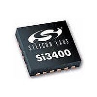
SI3402-A-GM Silicon Laboratories Inc, SI3402-A-GM Datasheet - Page 12

SI3402-A-GM
Manufacturer Part Number
SI3402-A-GM
Description
IC POE PD LOW EMI SW REG 20VQFN
Manufacturer
Silicon Laboratories Inc
Type
Power over Ethernet Switch (PoE)r
Datasheet
1.SI3402-A-GMR.pdf
(22 pages)
Specifications of SI3402-A-GM
Package / Case
20-VQFN
Applications
IP Phones, Power over LAN, Network Routers and Switches
Internal Switch(s)
Yes
Current Limit
470mA
Voltage - Supply
2.8 V ~ 57 V
Operating Temperature
-40°C ~ 85°C
Mounting Type
Surface Mount
Product
PoE / LAN Solutions
Supply Voltage (max)
57 V
Supply Voltage (min)
2.8 V
Power Dissipation
1.2 W
Operating Temperature Range
- 40 C to + 85 C
Mounting Style
SMD/SMT
Operating Temperature (min)
-40C
Operating Temperature Classification
Industrial
Operating Temperature (max)
85C
Rad Hardened
No
Lead Free Status / RoHS Status
Lead free / RoHS Compliant
Lead Free Status / RoHS Status
Lead free / RoHS Compliant, Lead free / RoHS Compliant
Available stocks
Company
Part Number
Manufacturer
Quantity
Price
Company:
Part Number:
SI3402-A-GM
Manufacturer:
SILICON
Quantity:
201
Company:
Part Number:
SI3402-A-GMR
Manufacturer:
DALLAS
Quantity:
101
Part Number:
SI3402-A-GMR
Manufacturer:
SILICON LABS/èٹ¯ç§‘
Quantity:
20 000
Si3402
3.2.1. Rectification Diode Bridges and
The 802.3 specification defines the input voltage at the
RJ-45 connector of the PD with no reference to polarity.
In other words, the PD must be able to accept power of
either polarity at each of its inputs. This requirement
necessitates the use of two sets of diode bridges, one
for the CT1 and CT2 pins and one for the SP1 and SP2
pins to rectify the voltage. Furthermore, the standard
requires that a PD withstand a high-voltage transient
surge consisting of a 1000 V common-mode impulse
with 300 ns rise time and 50 µs half fall time. Typically,
the diode bridge and the surge suppressor have been
implemented externally, adding cost and complexity to
the PD system design.
The diode bridge* and the surge suppressor have been
integrated into the Si3402, thus reducing system cost
and design complexity.
*Note: Silicon Laboratories recommends that on-chip diode
By integrating the diode bridges, the Si3402 gains
access to the input side of the diode bridge. Monitoring
the voltage at the input of the diode bridges instead of
the voltage across the load capacitor provides the
earliest indication of a power loss. This true early power
loss indicator, PLOSS, provides a local microcontroller
time to save states and shut down gracefully before the
load capacitor discharges below the minimum 802.3-
specified operating voltage of 36 V. Integration of the
surge suppressor enables optimization of the clamping
voltage and guarantees protection of all connected
circuitry.
12
(|CT1-CT2| or |SP1-SP2|)
57 down to 36 V
Surge Suppressor
bridges be bypassed when >10 W of output power is
required.
Input Voltage
Table 10. Hotswap Interface Modes
42 up to 57 V
2.7 to 11 V
14 to 22 V
22 to 42 V
11 to 14 V
0 to 2.7 V
Inactive
Detection turns off and
Switcher operating mode
Detection signature
internal bias starts
Classification signature
Transition region
(hysteresis limit based on
rising input voltage)
Switcher operating mode
(hysteresis limit based on
falling input voltage)
Si3402 Mode
Rev. 1.1
As an added benefit, the transient surge suppressor,
when tripped, actively disables the hotswap interface
and switching regulator, preventing downstream circuits
from encountering the high-energy transients.
3.2.2. Detection
In order to identify a device as a valid PD, a PSE will
apply a voltage in the range of 2.8 to 10 V on the cable
and look for the 25.5 k signature resistor. The Si3402
will react to voltages in this range by connecting an
external 25.5 k resistor between VPOS and VNEG.
This external resistor and internal low-leakage control
circuitry create the proper signature to alert the PSE
that a valid PD has been detected and is ready to have
power applied. The internal hotswap switch is disabled
during this time to prevent the switching regulator and
attached load circuitry from generating errors in the
detection signature.
Since the Si3402 integrates the diode bridges, the IC
can compensate for the voltage and resistance effects
of the diode bridges. The 802.3 specification requires
that the PSE use a multi-point, V/I measurement
technique to remove the diode-induced dc offset from
the signature resistance measurement. However, the
specification does not address the diode's nonlinear
resistance and the error induced in the signature
resistor measurement. Since the diode's resistance
appears in series with the signature resistor, the PD
system must find some way of compensating for this
error. In systems where the diode bridges are external,
compensation is difficult and suffers from errors. Since
the diode bridges are integrated in the Si3402, the IC
can compensate for this error by offsetting resistance
across all operating conditions and thus meeting the
802.3 requirements. An added benefit is that this
function can be tested during the IC’s automated testing
step, guaranteeing system compliance when used in
the final PD application. For more information about
supporting higher-power applications (above 12.95 W),
see “AN313: Using the Si3401/2 in High Power
Applications” and “AN314: Power Combining Circuit for
PoE for up to 18.5 W Output”.
3.2.3. Classification
Once the PSE has detected a valid PD, the PSE may
classify the PD for one of five power levels or classes. A
class is based on the expected power consumption of
the powered device. An external resistor sets the
nominal class current that can then be read by the PSE
to determine the proper power requirements of the PD.
When the PSE presents a fixed voltage between 15.5 V
and 20.5 V to the PD, the Si3402 asserts the class
current from VPOS through the RCL resistor. The
resistor values associated with each class are shown in
Table 11.


