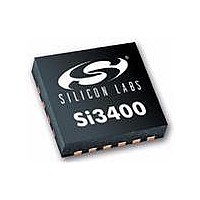
SI3402-A-GM Silicon Laboratories Inc, SI3402-A-GM Datasheet - Page 18

SI3402-A-GM
Manufacturer Part Number
SI3402-A-GM
Description
IC POE PD LOW EMI SW REG 20VQFN
Manufacturer
Silicon Laboratories Inc
Type
Power over Ethernet Switch (PoE)r
Datasheet
1.SI3402-A-GMR.pdf
(22 pages)
Specifications of SI3402-A-GM
Package / Case
20-VQFN
Applications
IP Phones, Power over LAN, Network Routers and Switches
Internal Switch(s)
Yes
Current Limit
470mA
Voltage - Supply
2.8 V ~ 57 V
Operating Temperature
-40°C ~ 85°C
Mounting Type
Surface Mount
Product
PoE / LAN Solutions
Supply Voltage (max)
57 V
Supply Voltage (min)
2.8 V
Power Dissipation
1.2 W
Operating Temperature Range
- 40 C to + 85 C
Mounting Style
SMD/SMT
Operating Temperature (min)
-40C
Operating Temperature Classification
Industrial
Operating Temperature (max)
85C
Rad Hardened
No
Lead Free Status / RoHS Status
Lead free / RoHS Compliant
Lead Free Status / RoHS Status
Lead free / RoHS Compliant, Lead free / RoHS Compliant
Available stocks
Company
Part Number
Manufacturer
Quantity
Price
Company:
Part Number:
SI3402-A-GM
Manufacturer:
SILICON
Quantity:
201
Company:
Part Number:
SI3402-A-GMR
Manufacturer:
DALLAS
Quantity:
101
Part Number:
SI3402-A-GMR
Manufacturer:
SILICON LABS/èٹ¯ç§‘
Quantity:
20 000
Si3402
6. Recommended Land Pattern
18
Notes:
General
Solder Mask Design
Stencil Design
Card Assembly
1. All dimensions shown are in millimeters (mm) unless otherwise noted.
2. Dimensioning and Tolerancing is per the ANSI Y14.5M-1994 specification.
3. This Land Pattern Design is based on the IPC-7351 guidelines.
4. All metal pads are to be non-solder mask defined (NSMD). Clearance between the solder mask and the
5. A stainless steel, laser-cut and electro-polished stencil with trapezoidal walls should be used to assure
6. The stencil thickness should be 0.125 mm (5 mils).
7. The ratio of stencil aperture to land pad size should be 1:1 for all perimeter pins.
8. A 2x2 array of 1.2 mm square openings on 1.4 mm pitch should be used for the center ground pad.
9. A No-Clean, Type-3 solder paste is recommended.
10. The recommended card reflow profile is per the JEDEC/IPC J-STD-020 specification for Small Body
metal pad is to be 60 µm minimum, all the way around the pad.
good solder paste release.
Components.
Symbol
P1
P2
X1
Y1
C1
C2
E
Figure 6. Si3402 Recommended Land Pattern
Table 14. PCB Land Pattern Dimensions
Min
2.70
2.70
0.25
0.90
Rev. 1.1
Nom
2.75
2.75
0.30
0.95
4.70
4.70
0.80
Max
2.80
2.80
0.35
1.00


