IRS26302DJPBF International Rectifier, IRS26302DJPBF Datasheet - Page 10
IRS26302DJPBF
Manufacturer Part Number
IRS26302DJPBF
Description
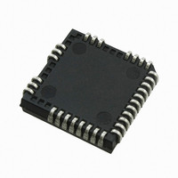
IC BRIDGE +1 GATE DVR 3PH 44PLCC
Manufacturer
International Rectifier
Datasheet
1.IRS26302DJTRPBF.pdf
(51 pages)
Specifications of IRS26302DJPBF
Configuration
3 Phase Bridge
Input Type
Non-Inverting
Delay Time
320ns
Current - Peak
200mA
Number Of Configurations
1
Number Of Outputs
3
High Side Voltage - Max (bootstrap)
600V
Voltage - Supply
10 V ~ 20 V
Operating Temperature
-40°C ~ 125°C
Mounting Type
Surface Mount
Package / Case
44-PLCC (32 Leads)
Number Of Drivers
6
Driver Configuration
Non-Inverting
Driver Type
High and Low Side
Input Logic Level
CMOS/TTL
Rise Time
190ns
Fall Time
75ns
Propagation Delay Time
710ns
Peak Output Current
350mA
Power Dissipation
4.6W
Operating Supply Voltage (min)
10V
Turn Off Delay Time
50ns
Turn On Delay Time (max)
50ns
Operating Temp Range
-40C to 125C
Operating Temperature Classification
Automotive
Mounting
Surface Mount
Pin Count
32
Package Type
PLCC
Lead Free Status / RoHS Status
Lead free / RoHS Compliant
Available stocks
Company
Part Number
Manufacturer
Quantity
Price
Company:

Part Number:
IRS26302DJPBF
Manufacturer:
International Rectifier
Quantity:
10 000


V
P
P
Dynamic Electrical Characteristics
LO
†
††
www.irf.com
LO
t
CC
Symbol
P
P
PFCbl
FCton
FCtoff
t
t
t
ITRIPBLK
LO
t
ITRIPOUT
LO
ITRIPFLT
t
t
HO
HO
FCtr
FCtf
t
FLTCLR
MDT
t
PFCtrip
= V
ITRIPbl
t
tr
filterEn
PM
tf
ITRIP
FILIN
MT
DT
t
EN
, HO
,HO
ton
toff
/B
/B
/B
/B
/t
ton
toff
The minimum width of the input pulse is recommended to exceed 500 ns to ensure the filtering time of the
input filter is exceeded.
PM is defined as PW
BRbl
B
Rton
Rtoff
Rtr
Rtf
,
,
= 15 V, V
tf
tr
Turn-on propagation delay, LO1,2,3,
HO1,2,3
Turn-off propagation delay, LO1,2,3,
HO1,2,3
Turn-on rise time LO1,2,3, HO1,2,3
Turn-off fall time LO1,2,3, HO1,2,3
Turn-on propagation delay,
PFC
(CL = 2200pF)
Turn-off propagation delay,
PFC
(CL = 2200pF)
Turn-on rise time, PFC
(CL= 2200 pF)
Turn-off rise time, PFC
= 2200 pF)
ENABLE low to output shutdown
propagation delay
ITRIP to output shutdown propagation
delay
ITRIP blanking time
PFC
propagation delay
PFC
Input filter time
/BR
Enable input filter time
Deadtime
Ton, off matching time (on all six
channels)
DT matching (Hi->Lo & Lo->Hi on all
channels)
Pulse width distortion
FAULT clear time RCIN: R=2meg,
C=1nF
ITRIP blanking time
ITRIP to fault time
ITRIP to output shutdown propagation
delay
S
IN
= V
OUT
OUT
TRIP
TRIP
, EN)
/BR
/BR
/BR
SS
to output shutdown
= COM, T
Definition
OUT
OUT
TRIP
IN
†
blanking time
- PW
(HIN, LIN, PFC
OUT
A
††
OUT
OUT
= 25
.
/BR
/BR
° C
OUT
OUT
, and C
IN
(CL
L
= 1000 pF unless otherwise specified.
Min
320
320
300
300
350
250
200
100
190
250
800
500
40
—
—
—
—
—
—
—
—
—
—
10
1150
Typ
125
180
460
800
400
800
500
350
200
290
400
720
50
60
60
—
—
—
—
—
—
—
1500
Max
710
710
190
660
660
650
600
420
600
950
75
50
60
75
80
—
—
—
—
—
—
—
Units
ns
µs
ns
LIN = 3.3 V
V
LIN = 0 V
V
© 2009 International Rectifier
LIN = 3.3 V
R = 100 K , C = 680 pF, on
ITRIP
ITRIP
V
IRS26302DJ
P
IN,
Test Conditions
P
=0 V
V
= 0 V
PW input = 10 us
V
FCIN
FCIN
C
C
V
IN
IN
C
C
EN
LOAD
LOAD
V
V
3.3 V
15 V
= 0 V or 3.3 V
= 0 V & 3.3 V
LOAD
LOAD
= 0 V
ITRIP
ITRIP
= 3.3 V
RCIN
= 0 V or 3.3 V
3.3 V
2 V to LOx/Hox =
3.3 V, HIN = 0 V
0 V, HIN = 0 V
= 2.2 nF
= 2.2 nF
2 V to FLT/En =
0 V, HIN = 0 V
= 1nF
= 1nF
= 2 V
= 2 V
0 V
0 V
3.3 V
0 V
Related parts for IRS26302DJPBF
Image
Part Number
Description
Manufacturer
Datasheet
Request
R

Part Number:
Description:
SCHOTTKY RECTIFIER
Manufacturer:
International Rectifier Corp.
Datasheet:
Part Number:
Description:
SCHOTTKY RECTIFIER
Manufacturer:
International Rectifier Corp.
Datasheet:
Part Number:
Description:
SCHOTTKY RECTIFIER
Manufacturer:
International Rectifier Corp.
Datasheet:
Part Number:
Description:
SCHOTTKY RECTIFIER
Manufacturer:
International Rectifier Corp.
Datasheet:
Part Number:
Description:
SCHOTTKY RECTIFIER
Manufacturer:
International Rectifier Corp.
Datasheet:
Part Number:
Description:
SCHOTTKY RECTIFIER
Manufacturer:
International Rectifier Corp.
Datasheet:
Part Number:
Description:
SCHOTTKY RECTIFIER
Manufacturer:
International Rectifier Corp.
Datasheet:
Part Number:
Description:
SCHOTTKY RECTIFIER
Manufacturer:
International Rectifier Corp.
Datasheet:
Part Number:
Description:
SCHOTTKY RECTIFIER
Manufacturer:
International Rectifier Corp.
Datasheet:
Part Number:
Description:
SCHOTTKY RECTIFIER
Manufacturer:
International Rectifier Corp.
Datasheet:
Part Number:
Description:
SCHOTTKY RECTIFIER
Manufacturer:
International Rectifier Corp.
Datasheet:
Part Number:
Description:
SCHOTTKY RECTIFIER
Manufacturer:
International Rectifier Corp.
Datasheet:
Part Number:
Description:
SCHOTTKY RECTIFIER
Manufacturer:
International Rectifier Corp.
Datasheet:
Part Number:
Description:
SCHOTTKY RECTIFIER
Manufacturer:
International Rectifier Corp.
Datasheet:
Part Number:
Description:
SCHOTTKY RECTIFIER
Manufacturer:
International Rectifier Corp.
Datasheet: