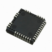
IRS26302DJPBF International Rectifier, IRS26302DJPBF Datasheet - Page 19

IRS26302DJPBF
Manufacturer Part Number
IRS26302DJPBF
Description
IC BRIDGE +1 GATE DVR 3PH 44PLCC
Manufacturer
International Rectifier
Datasheet
1.IRS26302DJTRPBF.pdf
(51 pages)
Specifications of IRS26302DJPBF
Configuration
3 Phase Bridge
Input Type
Non-Inverting
Delay Time
320ns
Current - Peak
200mA
Number Of Configurations
1
Number Of Outputs
3
High Side Voltage - Max (bootstrap)
600V
Voltage - Supply
10 V ~ 20 V
Operating Temperature
-40°C ~ 125°C
Mounting Type
Surface Mount
Package / Case
44-PLCC (32 Leads)
Number Of Drivers
6
Driver Configuration
Non-Inverting
Driver Type
High and Low Side
Input Logic Level
CMOS/TTL
Rise Time
190ns
Fall Time
75ns
Propagation Delay Time
710ns
Peak Output Current
350mA
Power Dissipation
4.6W
Operating Supply Voltage (min)
10V
Turn Off Delay Time
50ns
Turn On Delay Time (max)
50ns
Operating Temp Range
-40C to 125C
Operating Temperature Classification
Automotive
Mounting
Surface Mount
Pin Count
32
Package Type
PLCC
Lead Free Status / RoHS Status
Lead free / RoHS Compliant
Available stocks
Company
Part Number
Manufacturer
Quantity
Price
Company:
Part Number:
IRS26302DJPBF
Manufacturer:
International Rectifier
Quantity:
10 000
IRS26302DJ
Figure 7: Illustration of deadtime
Matched Propagation Delays
The IRS26302DJ is designed with propagation delay matching circuitry. With this feature, the IC’s response at the
output to a signal at the input requires approximately the same time duration (i.e., t
, t
) for both the low-side
ON
OFF
channels and the high-side channels; the maximum difference is specified by the delay matching parameter (MT).
Additionally, the propagation delay for each low-side channel is matched when compared to the other low-side
channels and the propagation delays of the high-side channels are matched with each other; the MT specification
applies as well. The propagation turn-on delay (t
) of the IRS26302DJ is matched to the propagation turn-on delay
ON
(t
).
OFF
Input Logic Compatibility
The inputs of this IC are compatible with standard CMOS and TTL outputs. The IRS26302DJ has been designed to
be compatible with 3.3 V and 5 V logic-level signals. Figure 8 illustrates an input signal to the IRS26302DJ, its input
threshold values, and the logic state of the IC as a result of the input signal.
Figure 8: HIN & LIN input thresholds
www.irf.com
© 2009 International Rectifier
19


