IRS26302DJPBF International Rectifier, IRS26302DJPBF Datasheet - Page 33
IRS26302DJPBF
Manufacturer Part Number
IRS26302DJPBF
Description
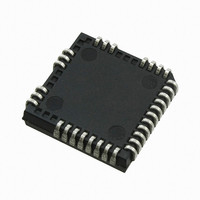
IC BRIDGE +1 GATE DVR 3PH 44PLCC
Manufacturer
International Rectifier
Datasheet
1.IRS26302DJTRPBF.pdf
(51 pages)
Specifications of IRS26302DJPBF
Configuration
3 Phase Bridge
Input Type
Non-Inverting
Delay Time
320ns
Current - Peak
200mA
Number Of Configurations
1
Number Of Outputs
3
High Side Voltage - Max (bootstrap)
600V
Voltage - Supply
10 V ~ 20 V
Operating Temperature
-40°C ~ 125°C
Mounting Type
Surface Mount
Package / Case
44-PLCC (32 Leads)
Number Of Drivers
6
Driver Configuration
Non-Inverting
Driver Type
High and Low Side
Input Logic Level
CMOS/TTL
Rise Time
190ns
Fall Time
75ns
Propagation Delay Time
710ns
Peak Output Current
350mA
Power Dissipation
4.6W
Operating Supply Voltage (min)
10V
Turn Off Delay Time
50ns
Turn On Delay Time (max)
50ns
Operating Temp Range
-40C to 125C
Operating Temperature Classification
Automotive
Mounting
Surface Mount
Pin Count
32
Package Type
PLCC
Lead Free Status / RoHS Status
Lead free / RoHS Compliant
Available stocks
Company
Part Number
Manufacturer
Quantity
Price
Company:

Part Number:
IRS26302DJPBF
Manufacturer:
International Rectifier
Quantity:
10 000


IRS26302DJ
PCB Layout Tips
Distance between high and low voltage components: It’s strongly recommended to place the components tied to the
floating voltage pins (V
and V
) near the respective high voltage portions of the device. The IRS26302DJ in the
B
S
PLCC44 package has had some unused pins removed in order to maximize the distance between the high voltage
and low voltage pins. Please see the Case Outline PLCC44 information in this datasheet for the details.
Ground Plane: In order to minimize noise coupling, the ground plane should not be placed under or near the high
voltage floating side.
Gate Drive Loops: Current loops behave like antennas and are able to receive and transmit EM noise (see Figure
36). In order to reduce the EM coupling and improve the power switch turn on/off performance, the gate drive loops
must be reduced as much as possible. Moreover, current can be injected inside the gate drive loop via the IGBT
collector-to-gate parasitic capacitance. The parasitic auto-inductance of the gate loop contributes to developing a
voltage across the gate-emitter, thus increasing the possibility of a self turn-on effect.
Figure 36: Antenna Loops
Supply Capacitor: It is recommended to place a bypass capacitor (C
) between the V
and V
pins. This
IN
CC
SS
connection is shown in Figure 37.
A ceramic 1
F ceramic capacitor is suitable for most applications. This
component should be placed as close as possible to the pins in order to reduce parasitic elements.
Figure 37: Supply capacitor
www.irf.com
© 2009 International Rectifier
33
Related parts for IRS26302DJPBF
Image
Part Number
Description
Manufacturer
Datasheet
Request
R

Part Number:
Description:
SCHOTTKY RECTIFIER
Manufacturer:
International Rectifier Corp.
Datasheet:
Part Number:
Description:
SCHOTTKY RECTIFIER
Manufacturer:
International Rectifier Corp.
Datasheet:
Part Number:
Description:
SCHOTTKY RECTIFIER
Manufacturer:
International Rectifier Corp.
Datasheet:
Part Number:
Description:
SCHOTTKY RECTIFIER
Manufacturer:
International Rectifier Corp.
Datasheet:
Part Number:
Description:
SCHOTTKY RECTIFIER
Manufacturer:
International Rectifier Corp.
Datasheet:
Part Number:
Description:
SCHOTTKY RECTIFIER
Manufacturer:
International Rectifier Corp.
Datasheet:
Part Number:
Description:
SCHOTTKY RECTIFIER
Manufacturer:
International Rectifier Corp.
Datasheet:
Part Number:
Description:
SCHOTTKY RECTIFIER
Manufacturer:
International Rectifier Corp.
Datasheet:
Part Number:
Description:
SCHOTTKY RECTIFIER
Manufacturer:
International Rectifier Corp.
Datasheet:
Part Number:
Description:
SCHOTTKY RECTIFIER
Manufacturer:
International Rectifier Corp.
Datasheet:
Part Number:
Description:
SCHOTTKY RECTIFIER
Manufacturer:
International Rectifier Corp.
Datasheet:
Part Number:
Description:
SCHOTTKY RECTIFIER
Manufacturer:
International Rectifier Corp.
Datasheet:
Part Number:
Description:
SCHOTTKY RECTIFIER
Manufacturer:
International Rectifier Corp.
Datasheet:
Part Number:
Description:
SCHOTTKY RECTIFIER
Manufacturer:
International Rectifier Corp.
Datasheet:
Part Number:
Description:
SCHOTTKY RECTIFIER
Manufacturer:
International Rectifier Corp.
Datasheet: