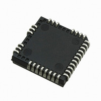
IRS26302DJPBF International Rectifier, IRS26302DJPBF Datasheet - Page 17

IRS26302DJPBF
Manufacturer Part Number
IRS26302DJPBF
Description
IC BRIDGE +1 GATE DVR 3PH 44PLCC
Manufacturer
International Rectifier
Datasheet
1.IRS26302DJTRPBF.pdf
(51 pages)
Specifications of IRS26302DJPBF
Configuration
3 Phase Bridge
Input Type
Non-Inverting
Delay Time
320ns
Current - Peak
200mA
Number Of Configurations
1
Number Of Outputs
3
High Side Voltage - Max (bootstrap)
600V
Voltage - Supply
10 V ~ 20 V
Operating Temperature
-40°C ~ 125°C
Mounting Type
Surface Mount
Package / Case
44-PLCC (32 Leads)
Number Of Drivers
6
Driver Configuration
Non-Inverting
Driver Type
High and Low Side
Input Logic Level
CMOS/TTL
Rise Time
190ns
Fall Time
75ns
Propagation Delay Time
710ns
Peak Output Current
350mA
Power Dissipation
4.6W
Operating Supply Voltage (min)
10V
Turn Off Delay Time
50ns
Turn On Delay Time (max)
50ns
Operating Temp Range
-40C to 125C
Operating Temperature Classification
Automotive
Mounting
Surface Mount
Pin Count
32
Package Type
PLCC
Lead Free Status / RoHS Status
Lead free / RoHS Compliant
Available stocks
Company
Part Number
Manufacturer
Quantity
Price
Company:
Part Number:
IRS26302DJPBF
Manufacturer:
International Rectifier
Quantity:
10 000
IRS26302DJ
Switching and Timing Relationships
The relationship between the input and output signals of the IRS26302DJ are illustrated below in Figures 3. From
this figure, we can see the definitions of several timing parameters (i.e., PW
, PW
, t
, t
, t
, and t
) associated
IN
OUT
ON
OFF
R
F
with this device.
Figure 3: Switching time waveforms
The following two figures illustrate the timing relationships of some of the functionality of the IRS26302DJ; this
functionality is described in further detail later in this document.
During interval A of Figure 5, the HVIC has received the command to turn-on both the high- and low-side switches at
the same time; as a result, the shoot-through protection of the HVIC has prevented this condition and both the high-
and low-side output are held in the off state.
Interval B of Figures 5 and 6 shows that the signal on the ITRIP, GF, PCFtrip input pin has gone from a not active to
an active state; as a result, all of the gate drive outputs have been disabled (i.e., see that HOx has returned to the low
state; LOx is also held low), the voltage on the RCIN pin has been pulled to 0 V, and a fault is reported by the FAULT
output transitioning to the low state. Once the ITRIP, GF, PCFtrip input has returned to the not active state, the
output will remain disabled and the fault condition reported until the voltage on the RCIN pin charges up to V
RCIN,TH
(see interval C in Figure 6); the charging characteristics are dictated by the RC network attached to the RCIN pin.
During intervals D and E of Figure 5, we can see that the enable (EN) pin has been pulled low (as is the case when
the driver IC has received a command from the control IC to shutdown); this results in the outputs (HOx and LOx)
being held in the low state until the enable pin is pulled high.
www.irf.com
© 2009 International Rectifier
17


