IRS26302DJPBF International Rectifier, IRS26302DJPBF Datasheet - Page 25
IRS26302DJPBF
Manufacturer Part Number
IRS26302DJPBF
Description
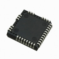
IC BRIDGE +1 GATE DVR 3PH 44PLCC
Manufacturer
International Rectifier
Datasheet
1.IRS26302DJTRPBF.pdf
(51 pages)
Specifications of IRS26302DJPBF
Configuration
3 Phase Bridge
Input Type
Non-Inverting
Delay Time
320ns
Current - Peak
200mA
Number Of Configurations
1
Number Of Outputs
3
High Side Voltage - Max (bootstrap)
600V
Voltage - Supply
10 V ~ 20 V
Operating Temperature
-40°C ~ 125°C
Mounting Type
Surface Mount
Package / Case
44-PLCC (32 Leads)
Number Of Drivers
6
Driver Configuration
Non-Inverting
Driver Type
High and Low Side
Input Logic Level
CMOS/TTL
Rise Time
190ns
Fall Time
75ns
Propagation Delay Time
710ns
Peak Output Current
350mA
Power Dissipation
4.6W
Operating Supply Voltage (min)
10V
Turn Off Delay Time
50ns
Turn On Delay Time (max)
50ns
Operating Temp Range
-40C to 125C
Operating Temperature Classification
Automotive
Mounting
Surface Mount
Pin Count
32
Package Type
PLCC
Lead Free Status / RoHS Status
Lead free / RoHS Compliant
Available stocks
Company
Part Number
Manufacturer
Quantity
Price
Company:

Part Number:
IRS26302DJPBF
Manufacturer:
International Rectifier
Quantity:
10 000


One FLT/EN pin and DIAG mode operation for all fault condition
Fault Diagnostic: DIAG STATE –State Diagram
After each fault event a diagnostic feature, if enable, can communicate to the controller which fault happened in the
system (UVcc, ITRIP, GF, PCFtrip). If diagnostic is enabled forcing all HIN and all LIN = High the HVIC enters in
handshake mode, all the outputs remain off, the automatic fault clear function is disabled and FLT/EN is in HZ (refer to
Figure 17 for more details). The HVIC fault register is now ready for queries. A procedure to interrogate the fault register
is depicted in the fault query routine (Figure 18).
(
(*) Operation available only in DIAL MODE.
(**) Internal Register fault
DIAG MODE available when FLT=0
Set DIAG MODE: Hinx=Linx=H
During DIAG MODE operation Lox=Hox=0 PFCout/BRout=0 RCIN=0
Reset DIAG MODE: hold Linx=H Hinx=L
www.irf.com
0
) HAND SHAKE SYNC
Lin1=L Lin2, 3=H
Lin1=L Lin2, 3=H
Lin2=L Lin1, 3=H
Lin2=L Lin1, 3=H
Lin3=L Lin1,2=H
Lin3=L Lin1,2=H
Lin1,2=L Lin3=H
Lin1,2=L Lin3=H
LIN1,2,3
ALL=H
Linx
Linx
Linx
Linx
Linx
HIN1,2
ALL H
ALL H
ALL H
ALL H
ALL H
ALL H
ALL H
ALL H
ALL H
Hinx
Hinx
Hinx
Hinx
Hinx
,3
PFCinx/BRinx
PFCinx/BRinx
PFCinx/BRinx
PFCinx/BRinx
PFCinx/BRinx
PFCinx/BRinx
PFCinx/BRinx
PFCinx/BRinx
PFCinx/BRinx
PFCinx/BRinx
PFCinx/BRinx
PFCinx/BRinx
PFCinx/BRinx
PFCinx/BRinx
PFCin/BRin
Condi
tion
(
(*)
(*)
(*)
(*)
(*)
(*)
(*)
(*)
0
)
RCIN
HZ
HZ
HZ
0
0
0
0
0
0
0
0
0
0
0
Figure 17: State Diagram
V > Vth (**)
V > Vth (**)
Itrip
X
X
X
X
X
X
X
X
X
0
0
25
V > Vth (**)
V > Vth (**)
PFCtrip
Fault register = 1 (**)
0
X
X
X
0
X
X
X
X
X
X
V > Vth (**)
V > Vth (**)
GF
X
X
X
X
X
X
X
X
X
0
V
V
V
V
VCC fault
CC
CC
CC
CC
> UV
< UV
< UV
> UV
X
X
X
X
X
X
X
X
X
CC
CC
CC
CC
0-> HZ (
EN/FLT
© 2009 International Rectifier
HZ
HZ
HZ
HZ
HZ
0
0
0
0
0
0
0
0
IRS26302DJ
0
)
Lox
0
0
0
0
0
0
0
0
0
0
0
0
0
Hox
0
0
0
0
0
0
0
0
0
0
0
0
0
PFCout/
BRout
0
0
0
0
0
0
0
0
0
0
0
0
0
Related parts for IRS26302DJPBF
Image
Part Number
Description
Manufacturer
Datasheet
Request
R

Part Number:
Description:
SCHOTTKY RECTIFIER
Manufacturer:
International Rectifier Corp.
Datasheet:
Part Number:
Description:
SCHOTTKY RECTIFIER
Manufacturer:
International Rectifier Corp.
Datasheet:
Part Number:
Description:
SCHOTTKY RECTIFIER
Manufacturer:
International Rectifier Corp.
Datasheet:
Part Number:
Description:
SCHOTTKY RECTIFIER
Manufacturer:
International Rectifier Corp.
Datasheet:
Part Number:
Description:
SCHOTTKY RECTIFIER
Manufacturer:
International Rectifier Corp.
Datasheet:
Part Number:
Description:
SCHOTTKY RECTIFIER
Manufacturer:
International Rectifier Corp.
Datasheet:
Part Number:
Description:
SCHOTTKY RECTIFIER
Manufacturer:
International Rectifier Corp.
Datasheet:
Part Number:
Description:
SCHOTTKY RECTIFIER
Manufacturer:
International Rectifier Corp.
Datasheet:
Part Number:
Description:
SCHOTTKY RECTIFIER
Manufacturer:
International Rectifier Corp.
Datasheet:
Part Number:
Description:
SCHOTTKY RECTIFIER
Manufacturer:
International Rectifier Corp.
Datasheet:
Part Number:
Description:
SCHOTTKY RECTIFIER
Manufacturer:
International Rectifier Corp.
Datasheet:
Part Number:
Description:
SCHOTTKY RECTIFIER
Manufacturer:
International Rectifier Corp.
Datasheet:
Part Number:
Description:
SCHOTTKY RECTIFIER
Manufacturer:
International Rectifier Corp.
Datasheet:
Part Number:
Description:
SCHOTTKY RECTIFIER
Manufacturer:
International Rectifier Corp.
Datasheet:
Part Number:
Description:
SCHOTTKY RECTIFIER
Manufacturer:
International Rectifier Corp.
Datasheet: