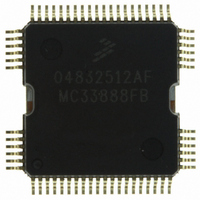
MC33888FB Freescale Semiconductor, MC33888FB Datasheet - Page 15

MC33888FB
Manufacturer Part Number
MC33888FB
Description
IC SWITCH QUAD H-SIDE W/CS 64QFP
Manufacturer
Freescale Semiconductor
Type
High Side/Low Side Driverr
Datasheet
1.MC33888FBR2.pdf
(40 pages)
Specifications of MC33888FB
Input Type
SPI
Number Of Outputs
12 ( 4 High Side, 8 Low Side)
On-state Resistance
40 mOhm
Current - Output / Channel
10A
Current - Peak Output
60A
Voltage - Supply
6 V ~ 27 V
Operating Temperature
-40°C ~ 125°C
Mounting Type
Surface Mount
Package / Case
64-QFP
Lead Free Status / RoHS Status
Lead free / RoHS Compliant
Available stocks
Company
Part Number
Manufacturer
Quantity
Price
Company:
Part Number:
MC33888FB
Manufacturer:
GPS
Quantity:
6 218
Company:
Part Number:
MC33888FB
Manufacturer:
Freescale Semiconductor
Quantity:
10 000
Part Number:
MC33888FB
Manufacturer:
MOTOROLA/摩托罗拉
Quantity:
20 000
Company:
Part Number:
MC33888FBR2
Manufacturer:
Freescale Semiconductor
Quantity:
10 000
Part Number:
MC33888FBR2
Manufacturer:
FREESCALE
Quantity:
20 000
Table 6. Dynamic Electrical Characteristics
Typical values noted reflect the approximate parameter means at T
Analog Integrated Circuit Device Data
Freescale Semiconductor
POWER OUTPUT TIMING
Notes
High-Side Output Rising Fast Slew Rate
High-Side Output Rising Slow Slew Rate
High-Side Output Falling Fast Slew Rate
High-Side Output Falling Slow Slew Rate
High-Side Output Turn ON Delay Time
High-Side Output Turn OFF Delay Time
Low-Side Output Falling Slew Rate
Low-Side Output Rising Slew Rate
Low-Side Output Turn ON Delay Time
Low-Side Output Turn OFF Delay Time
Low-Side Output Fault Delay Timer
27.
28.
29.
30.
31.
32.
33.
34.
Characteristics noted under conditions 6.0 V ≤ V
6.0 V < V
9.0 V < V
16 V < V
6.0 V < V
9.0 V < V
16 V < V
6.0 V < V
9.0 V < V
16 V < V
6.0 V < V
9.0 V < V
16 V < V
High-side output rise and fall fast slew rates measured across a 5.0 Ω resistive load at high-side output = 0.5 V to V
(see
High-side output rise and fall slow slew rates measured across a 5.0 Ω resistive load at high-side output = 0.5 V to V
(see
High-side output turn-ON delay time measured from 50% of the rising IHS to 0.5 V of output OFF with R
(see
High-side output turn-OFF delay time measured from 50% of the falling IHS to V
load (see
Low-side output rise and fall slew rates measured across a 5.0 Ω resistive load at low-side output = 10% to 90% (see
Low-side output turn-ON delay time measured from 50% of the rising ILS to 90% of V
page 17).
Low-side output turn-OFF delay time measured from 50% of the falling ILS to 10% of V
page 17). These parameters are guaranteed by process monitoring.
Propagation time of Short Fault Disable Report Delay measured from rising edge of CS to output disabled, low-side = 5.0 V, and device
configured for low-side output overcurrent latch-off using CLOCCR.
Figure
Figure
Figure
PWR
PWR
PWR
PWR
PWR
PWR
PWR
PWR
PWR
PWR
PWR
PWR
Figure
< 27 V
< 27 V
< 27 V
< 27 V
< 9.0 V
< 16 V
< 9.0 V
< 16 V
< 9.0 V
< 16 V
< 9.0 V
< 16 V
5, page 17). These parameters are guaranteed by process monitoring.
5, page 17). These parameters are guaranteed by process monitoring.
5, page 17).
5, page 17).
Characteristic
(31)
(31)
(34)
(32)
(29)
DYNAMIC ELECTRICAL CHARACTERISTICS
(33)
(30)
(27)
(27)
(28)
(28)
PWR
≤ 27 V, 4.5 V ≤ V
A
= 25°C under nominal conditions unless otherwise noted.
DD
SR
SR
SR
SR
t
t
t
t
Symbol
t
DLY(OFF)
DLY(OFF)
DLY(ON)
DLY(ON)
DLY(
R_SLOW
F_SLOW
≤ 5.5 V, -40°C ≤ T
SR
SR
R_FAST
F_FAST
F
R
FS
PWR
)
- 2.0 V of the output OFF with R
OUT
OUT
DYNAMIC ELECTRICAL CHARACTERISTICS
0.03
0.05
0.01
0.01
0.01
0.05
0.08
0.08
Min
with R
0.1
0.2
0.3
0.5
5.0
5.0
0.5
1.0
0.5
0.5
70
with R
L
J
L
= 27 Ω resistive load (see
≤ 150°C unless otherwise noted.
= 27 Ω resistive load (see
0.08
0.15
Typ
150
0.5
0.8
3.0
6.0
2.0
4.0
ELECTRICAL CONNECTIONS
30
80
–
–
–
–
–
–
–
–
L
= 27 Ω resistive load
Max
0.14
0.18
150
150
250
0.6
0.8
1.1
0.2
1.0
1.5
2.2
0.3
0.4
0.5
10
20
10
10
Figure
PWR
L
PWR
= 27 Ω resistive
- 3.0 V
- 3.0 V
6, page 17).
Figure
Figure
Unit
V/µs
V/µs
V/µs
V/µs
V/µs
V/µs
µs
µs
µs
µs
µs
33888
6,
6,
15


