MC33888FB Freescale Semiconductor, MC33888FB Datasheet - Page 20
MC33888FB
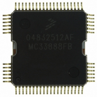
Manufacturer Part Number
MC33888FB
Description
IC SWITCH QUAD H-SIDE W/CS 64QFP
Manufacturer
Freescale Semiconductor
Type
High Side/Low Side Driverr
Datasheet
1.MC33888FBR2.pdf
(40 pages)
Specifications of MC33888FB
Input Type
SPI
Number Of Outputs
12 ( 4 High Side, 8 Low Side)
On-state Resistance
40 mOhm
Current - Output / Channel
10A
Current - Peak Output
60A
Voltage - Supply
6 V ~ 27 V
Operating Temperature
-40°C ~ 125°C
Mounting Type
Surface Mount
Package / Case
64-QFP
Lead Free Status / RoHS Status
Lead free / RoHS Compliant
Available stocks
Company
Part Number
Manufacturer
Quantity
Price
Company:

Part Number:
MC33888FB
Manufacturer:
GPS
Quantity:
6 218
Company:
Part Number:
MC33888FB
Manufacturer:
Freescale Semiconductor
Quantity:
10 000
Part Number:
MC33888FB
Manufacturer:
MOTOROLA/摩托罗拉
Quantity:
20 000
Company:
Part Number:
MC33888FBR2
Manufacturer:
Freescale Semiconductor
Quantity:
10 000
Part Number:
MC33888FBR2
Manufacturer:
FREESCALE
Quantity:
20 000


WATCHDOG AND FAIL-SAFE OPERATION
WAKE or RST transitions from logic [0] to logic [1]. The
WAKE input is capable of being pulled up to V
series limiting resistance that limits the internal clamp current.
The timeout is a multiple of an internal oscillator. As long as
the WDIN pin or the WD bit (D15) of an incoming SPI
message is toggled within the minimum watchdog timeout,
WDTO (or a divided value configured during a WDCSCR
message), then the device will operate normally. If the
watchdog timeout occurs before the WD bit or the WDIN pin
is toggled, then the device will revert to a Fail-Safe mode until
the device is re initialized (if the FSI pin is left disconnected).
HS0 and HS2, which will be driven ON regardless of the state
of the various direct inputs and modes
can be brought out of the Fail-Safe mode by transitioning the
WAKE and RST pins from logic [1] to logic [0]. In the event
the WAKE pin was not transitioned to a logic [1] during
normal operation and the watchdog times out, then the
device can be brought out of fail-safe by bringing the RST to
a logic [0]. If the FSI pin is tied to GND, then the watchdog,
and therefore fail-safe operation, will be disabled.
DEFAULT MODE
first applying V
to logic [1] prior to SPI communication. In the default mode,
all outputs will be off (assuming that the direct inputs ILS and
IHS[0:3] and the WAKE pin are at logic [0] ). All of the specific
pin functions will operate as though all of the addressable
configuration register bits were set to logic [0]. This means,
for example, that all of the low-side outputs will be
controllable by the ILS pin, and that all high-side outputs will
be controllable via their respective IHS pins. During the
default mode, all high-side drivers will default with open load
detection enabled. All low-side drivers will default with open
load detection disabled. This mode allows limited control of
the 33888 with the direct inputs in the absence of an SPI.
normal operation, followed by the removal of the V
voltage, requires that the RST input be held at a logic [0] state
until V
input levels are normal, then failure to allow V
below 2.0 V will result in an internal bias circuit clamping the
V
2.0 V, the RST can be returned to 5.0 V without re-enabling
the bias circuit.
20
33888
FUNCTIONAL DEVICE OPERATION
OPERATIONAL MODES
PWR
The watchdog is enabled and a timeout is started when the
During Fail-Safe mode, all outputs will be OFF except for
The default mode describes the state of the device after
Returning the device to the default state after a period of
PWR
pin to approximately 3.5 V. Once V
falls to a level below 2.0 V. If the RST and V
PWR
voltage or a reset transition from logic [0]
FUNCTIONAL DEVICE OPERATION
(Table
PWR
7). The device
PWR
PWR
falls below
OPERATIONAL MODES
PWR
to fall
with a
DD
FAULT LOGIC REQUIREMENTS
occur:
output specific. The overvoltage fault is a global fault. The
overcurrent fault is only reported for the low-side outputs.
filter, t
transients for overcurrent faults when the output is ON and
open load faults when the output is OFF. All faults are latched
and indicated by a logic [1] for each output in the 33888
status word
status bit for the faulted output will be cleared by a rising edge
on CS.
Table 7. Fail-Safe Operation and Transitions to Other
WAKE
Assumptions: Normal operating voltage and junction temperatures,
FSI pin floating.
x = Don’t care.
S = State determined by SPI and/or direct input configurations.
The 33888 indicates all of the following faults as they
• Overtemperature Fault
• Overvoltage Fault
• Open Load Fault
• Overcurrent Fault
With the exception of the overvoltage, these faults are
The 33888 low-side outputs incorporate an internal fault
0
1
1
0
0
1
1
DLY(
RS
T
0
0
0
1
1
1
1
FS
33888 Modes
WDTO HS0 HS2
(Table
)
. The fault timer filters noise and switching
YES
YES
YES
NO
NO
NO
x
10, page 25). If the fault is removed, the
OF
OF
ON ON
ON ON
ON ON
F
F
S
S
Analog Integrated Circuit Device Data
OF
OF
F
F
S
S
LS[4:11],
HS[1,3]
OFF
OFF
OFF
OFF
OFF
S
S
Freescale Semiconductor
Device in Sleep mode.
All outputs are OFF.
When
logic [1], device is in
default.
Fail-Safe mode. Device
reset into Default mode
by transitioning WAKE
to logic [0].
Device in Normal
operating mode.
Fail-Safe mode. Device
reset into Default mode
by transitioning
logic [0].
Device in Normal
operating mode.
Fail-Safe mode. Device
reset into Default mode
by transitioning
and WAKE to logic [0].
Comments
RST
transitions to
RST
RST
to
Related parts for MC33888FB
Image
Part Number
Description
Manufacturer
Datasheet
Request
R

Part Number:
Description:
Manufacturer:
Freescale Semiconductor, Inc
Datasheet:
Part Number:
Description:
Manufacturer:
Freescale Semiconductor, Inc
Datasheet:
Part Number:
Description:
Manufacturer:
Freescale Semiconductor, Inc
Datasheet:
Part Number:
Description:
Manufacturer:
Freescale Semiconductor, Inc
Datasheet:
Part Number:
Description:
Manufacturer:
Freescale Semiconductor, Inc
Datasheet:
Part Number:
Description:
Manufacturer:
Freescale Semiconductor, Inc
Datasheet:
Part Number:
Description:
Manufacturer:
Freescale Semiconductor, Inc
Datasheet:
Part Number:
Description:
Manufacturer:
Freescale Semiconductor, Inc
Datasheet:
Part Number:
Description:
Manufacturer:
Freescale Semiconductor, Inc
Datasheet:
Part Number:
Description:
Manufacturer:
Freescale Semiconductor, Inc
Datasheet:
Part Number:
Description:
Manufacturer:
Freescale Semiconductor, Inc
Datasheet:
Part Number:
Description:
Manufacturer:
Freescale Semiconductor, Inc
Datasheet:
Part Number:
Description:
Manufacturer:
Freescale Semiconductor, Inc
Datasheet:
Part Number:
Description:
Manufacturer:
Freescale Semiconductor, Inc
Datasheet:
Part Number:
Description:
Manufacturer:
Freescale Semiconductor, Inc
Datasheet: