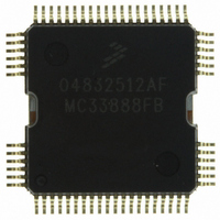
MC33888FB Freescale Semiconductor, MC33888FB Datasheet - Page 27

MC33888FB
Manufacturer Part Number
MC33888FB
Description
IC SWITCH QUAD H-SIDE W/CS 64QFP
Manufacturer
Freescale Semiconductor
Type
High Side/Low Side Driverr
Datasheet
1.MC33888FBR2.pdf
(40 pages)
Specifications of MC33888FB
Input Type
SPI
Number Of Outputs
12 ( 4 High Side, 8 Low Side)
On-state Resistance
40 mOhm
Current - Output / Channel
10A
Current - Peak Output
60A
Voltage - Supply
6 V ~ 27 V
Operating Temperature
-40°C ~ 125°C
Mounting Type
Surface Mount
Package / Case
64-QFP
Lead Free Status / RoHS Status
Lead free / RoHS Compliant
Available stocks
Company
Part Number
Manufacturer
Quantity
Price
Company:
Part Number:
MC33888FB
Manufacturer:
GPS
Quantity:
6 218
Company:
Part Number:
MC33888FB
Manufacturer:
Freescale Semiconductor
Quantity:
10 000
Part Number:
MC33888FB
Manufacturer:
MOTOROLA/摩托罗拉
Quantity:
20 000
Company:
Part Number:
MC33888FBR2
Manufacturer:
Freescale Semiconductor
Quantity:
10 000
Part Number:
MC33888FBR2
Manufacturer:
FREESCALE
Quantity:
20 000
UNDERVOLTAGE SHUTDOWN REQUIREMENTS
For the A version, the low side shutdown at a lower value,
V
internal logic states within the device are designed to be
sustained. This ensures that when the battery level then rises
above 6.0 V, the device will return to the state that it was in
prior to the excursion between 5.0 V and 6.0 V (assuming
that there was no SPI communication or direct input changes
during the event). If the battery voltage falls to a level below
5.0 V, then the internal logic is re initialized and the device is
then in the default state upon the return of levels in excess of
6.0 V.
OUTPUT VOLTAGE CLAMPING
and dissipate the energy stored in inductive loads. Each
clamp independently limits the drain-to-source voltage to the
range specified in the Power Outputs section of
Static Electrical Characteristics
see
Analog Integrated Circuit Device Data
Freescale Semiconductor
PWRUV
All outputs turn off at some battery voltage below 6.0 V;
Each output has an internal clamp to provide protection
Figure
. however, as long as the level stays above 5.0 V, the
11.
Figure 10. Low-Side Short Circuit Detection and Analog Current Limit
beginning on page 10. Also
HIGH = Fault
Analog
V
THRES
Digital
+
–
Table 5,
V
+
V
–
2.0 V–4.0 V
OFD(THRES)LS
REF
33888
resistive or capacitive loads, but additional protection circuitry
is required for the device to support a battery disconnect for
an inductive load connected to HS pins.
GND
MOSFET ON
Drain-Source
ON Voltage
(V
Drain Current
(I
If the VPWR supply is disconnected, no issue exists for
D
DS(ON)
= 0.5 A)
Drain-Source
Clamp Voltage
(V
Figure 11. Low-Side Output Voltage Clamping
CL
)
= 53 V)
PROTECTION AND DIAGNOSTIC FEATURES
V
Current
Area (I
R
PWR
L
OUT
FUNCTIONAL DEVICE OPERATION
A
)
Drain Voltage
Clamp Energy
(E
J
= I
A
x V
CL
VPWR
x t)
Time
33888
27


