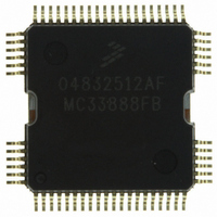
MC33888FB Freescale Semiconductor, MC33888FB Datasheet - Page 19

MC33888FB
Manufacturer Part Number
MC33888FB
Description
IC SWITCH QUAD H-SIDE W/CS 64QFP
Manufacturer
Freescale Semiconductor
Type
High Side/Low Side Driverr
Datasheet
1.MC33888FBR2.pdf
(40 pages)
Specifications of MC33888FB
Input Type
SPI
Number Of Outputs
12 ( 4 High Side, 8 Low Side)
On-state Resistance
40 mOhm
Current - Output / Channel
10A
Current - Peak Output
60A
Voltage - Supply
6 V ~ 27 V
Operating Temperature
-40°C ~ 125°C
Mounting Type
Surface Mount
Package / Case
64-QFP
Lead Free Status / RoHS Status
Lead free / RoHS Compliant
Available stocks
Company
Part Number
Manufacturer
Quantity
Price
Company:
Part Number:
MC33888FB
Manufacturer:
GPS
Quantity:
6 218
Company:
Part Number:
MC33888FB
Manufacturer:
Freescale Semiconductor
Quantity:
10 000
Part Number:
MC33888FB
Manufacturer:
MOTOROLA/摩托罗拉
Quantity:
20 000
Company:
Part Number:
MC33888FBR2
Manufacturer:
Freescale Semiconductor
Quantity:
10 000
Part Number:
MC33888FBR2
Manufacturer:
FREESCALE
Quantity:
20 000
HIGH-SIDE INPUT (IHS3, IHS2, IHS0, IHS1)
designated high-side output. These inputs may or may not be
activated depending on the configured state of the internal
logic.
CURRENT SENSE (2-3, 0-1)
output current that can be used to generate signal ground
referenced output voltages for use by the MCU. Each
respective CSNS pin can be configured via SPI to deliver
current from either of the two assigned outputs, or the
currents could be the sum of the two. Current from HS0 and/
or HS1 are sensed via CSNS0 - 1. Current from HS2 and/or
HS3 are sensed via CSNS2 - 3.
HIGH SIDE OUTPUT (HS3, HS2)
driver, which delivers current through the connected loads.
These outputs can be controlled via SPI or using the IHS pins
depending on the internal configuration. These outputs are
current limited and thermally protected. During fail-safe
mode, output HS2 will be turned on until the device is re-
initialized and then immediately followed by normal
operation.
HIGH SIDE OUTPUT (HS1, HS0)
driver, which delivers current through the connected loads.
These outputs can be controlled via SPI or using the IHS pins
depending on the internal configuration. These outputs are
current limited and thermally protected. During fail-safe
mode, output HS0 will be turned on until the device is re
Analog Integrated Circuit Device Data
Freescale Semiconductor
Each high-side input pin is used to directly control only one
These pins deliver a metered amount of the high-side
Each pin is the source of a 40 mΩ MOSFET high-side
Each pin is the source of a 10 mΩ MOSFET high-side
initialized and then immediately followed by normal
operation.
WAKE (WAKE)
the watchdog timer function. An internal clamp protects the
pin from high voltages when current is limited with an external
resistor. This input has a passive internal pulldown.
RESET (RST)
and fault registers, as well as place the device in a low current
standby mode. This pin also starts the watchdog timeout
when transitioned from logic [0] to logic [1]. This pin should
not be allowed to be at logic [1] until V
input has an internal passive pulldown.
FAIL-SAFE INPUT (FSI)
outputs after a watchdog timeout occurs. This pin has an
internal pullup. If the FSI pin is left to float to a logic [1], then
HS0 and HS2 will turn on when in the Fail-Safe state. If the
FSI pin is tied to GND, the watchdog circuit and fail-safe
operation will be disabled, thus allowing operation without a
watchdog signal.
WATCHDOG INPUT (WDIN)
monitor system operation. If the incoming watchdog signal
does not transition within the normal watchdog timeout
range, the device will operate in the Fail-Safe mode. This
input has an active internal pulldown.
This pin is used to input a logic [1] signal in order to enable
This input pin is used to initialize the device configuration
The Fail-Safe input pin level determines the state of the
This input pin is a CMOS logic level input that is used to
FUNCTIONAL PIN DESCRIPTION
FUNCTIONAL DESCRIPTION
DD
is in regulation. This
33888
19


