LM96194CISQ/NOPB National Semiconductor, LM96194CISQ/NOPB Datasheet - Page 103
LM96194CISQ/NOPB
Manufacturer Part Number
LM96194CISQ/NOPB
Description
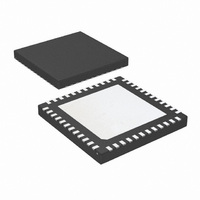
IC TRUTHERM HDWR MONITOR 48-LLP
Manufacturer
National Semiconductor
Series
PowerWise®, TruTherm®r
Datasheet
1.LM96194CISQNOPB.pdf
(106 pages)
Specifications of LM96194CISQ/NOPB
Function
Fan Control, Temp Monitor
Topology
ADC (Sigma Delta), Comparator, Fan Control, Multiplexer, Register Bank
Sensor Type
External & Internal
Sensing Temperature
-40°C ~ 85°C, External Sensor
Output Type
SMBus™
Output Alarm
No
Output Fan
Yes
Voltage - Supply
3 V ~ 3.6 V
Operating Temperature
-40°C ~ 85°C
Mounting Type
Surface Mount
Package / Case
48-LLP
Lead Free Status / RoHS Status
Lead free / RoHS Compliant
Other names
LM96194CISQTR


AD_IN4
AD_IN5
GND
GND
GND
AD_IN6
AD_IN7
AD_IN8
ADDR_SEL
AD_IN9/V
GND
PWM1
PWM2
P1_VID0
P1_VID1
P1_VID2
P1_VID3
P1_VID4
P1_VID5
Note 4: Human body model, 100 pF discharged through a 1.5 kΩ resistor. Machine model, 200 pF discharged directly into each pin. Charged device model (CDM)
simulates a pin slowly acquiring charge (such as from a device sliding down the feeder in an automated assembler) then rapidly being discharged.
Note 5: Reflow temperature profiles are different for lead-free and non lead-free packages.
Note 6: The maximum power dissipation must be de-rated at elevated temperatures and is dictated by T
allowable power dissipation at any temperature is P
air flow is listed in the following table.
Note 7: See the URL "http://www.national.com/packaging/" for other recommendations and methods of soldering surface mount devices.
Note 8: At the time of first pubication of this specification (Jan 2006), this specification applies to either Pentium or Xeon Processors on 90nm or 65nm process
when TruTherm is selected. When TruTherm is deselected this specification applies to an MMBT3904. This specification does include the error caused by the
variability of the diode ideality and series resistance parameters.
Note 9: Typical parameters are at T
Note 10: Limits are guaranteed to National's AOQL (Average Outgoing Quality Level).
Note 11: TUE (Total Unadjusted Error) includes Offset, Gain and Linearity errors of the ADC.
Note 12: Total Monitoring Cycle Time includes all temperature and voltage conversions.
Note 13: Leakage current approximately doubles every 20 °C.
Note 14: A total digital I/O current of 40 mA can cause 6 mV of offset in Vref.
Note 15: Timing specifications are tested at the TTL logic levels, V
to 1.4V.
DD
(V+)
Symbol
1.14 m/s (225 LFPM)
2.54 m/s (500 LFPM)
Air Flow
J
0 m/s
= T
A
= 25 °C and represent most likely parametric norm.
D MAX
Pin #
30
31
32
33
34
35
36
37
38
39
40
41
42
43
44
45
46
47
48
= (T
JMAX
shorted to AGND.)
− T
B (Internally
IL
= 0.4V for a falling edge and V
Circuit
A
) / θ
E
E
E
E
E
E
E
D
A
B
A
A
A
A
A
A
A
A
JA
. The θ
103
JA
Circuit D
Circuit E
for the LM96194 when mounted to 1 oz. copper foil PCB the θ
Junction to Ambient Thermal Resistance, θ
IH
= 2.4V for a rising edge. TRI-STATE output voltage is forced
JMAX
, θ
JA
and the ambient temperature, T
All Input Circuits
28 °C/W
25 °C/W
22 °C/W
JA
A
. The maximum
JA
www.national.com
with different
Related parts for LM96194CISQ/NOPB
Image
Part Number
Description
Manufacturer
Datasheet
Request
R

Part Number:
Description:
National Semiconductor [8-Bit D/A Converter]
Manufacturer:
National Semiconductor
Datasheet:
Part Number:
Description:
National Semiconductor [Media Coprocessor]
Manufacturer:
National Semiconductor
Datasheet:
Part Number:
Description:
Digitally Controlled Tone and Volume Circuit with Stereo Audio Power Amplifier, Microphone Preamp Stage and National 3D Sound
Manufacturer:
National Semiconductor
Datasheet:
Part Number:
Description:
Digitally Controlled Tone and Volume Circuit with Stereo Audio Power Amplifier, Microphone Preamp Stage and National 3D Sound
Manufacturer:
National Semiconductor
Datasheet:
Part Number:
Description:
AC97 Rev 2 Codec with Sample Rate Conversion and National 3D Sound
Manufacturer:
National Semiconductor
Part Number:
Description:
Manufacturer:
National Semiconductor
Datasheet:
Part Number:
Description:
Manufacturer:
National Semiconductor
Datasheet:
Part Number:
Description:
General Purpose, Low Voltage, Low Power, Rail-to-Rail Output Operational Amplifiers
Manufacturer:
National Semiconductor
Datasheet:
Part Number:
Description:
8-bit 20 MSPS flash A/D converter.
Manufacturer:
National Semiconductor
Datasheet:
Part Number:
Description:
Low Noise Quad Operational Amplifier
Manufacturer:
National Semiconductor
Datasheet:
Part Number:
Description:
Quad Differential Line Receivers
Manufacturer:
National Semiconductor
Datasheet:
Part Number:
Description:
Quad High Speed Trapezoidal? Bus Transceiver
Manufacturer:
National Semiconductor
Datasheet:
Part Number:
Description:
Dual Line Receiver
Manufacturer:
National Semiconductor
Datasheet:
Part Number:
Description:
TTL to 10k ECL Level Translator with Latch
Manufacturer:
National Semiconductor
Datasheet: