LM96194CISQ/NOPB National Semiconductor, LM96194CISQ/NOPB Datasheet - Page 26
LM96194CISQ/NOPB
Manufacturer Part Number
LM96194CISQ/NOPB
Description
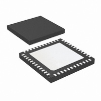
IC TRUTHERM HDWR MONITOR 48-LLP
Manufacturer
National Semiconductor
Series
PowerWise®, TruTherm®r
Datasheet
1.LM96194CISQNOPB.pdf
(106 pages)
Specifications of LM96194CISQ/NOPB
Function
Fan Control, Temp Monitor
Topology
ADC (Sigma Delta), Comparator, Fan Control, Multiplexer, Register Bank
Sensor Type
External & Internal
Sensing Temperature
-40°C ~ 85°C, External Sensor
Output Type
SMBus™
Output Alarm
No
Output Fan
Yes
Voltage - Supply
3 V ~ 3.6 V
Operating Temperature
-40°C ~ 85°C
Mounting Type
Surface Mount
Package / Case
48-LLP
Lead Free Status / RoHS Status
Lead free / RoHS Compliant
Other names
LM96194CISQTR


www.national.com
The board designer may apply a 10 kΩ pull-down and/or pull-
up resistors to ground and/or to 3.3V SB V
ADDR_SEL pin. The LM96194 is designed to work with re-
sistors of 5% tolerance for the case where two resistors are
15.4 DEVICE SETUP
BIOS executes the following steps to configure the registers
in the LM96194. All steps may not be necessary if default
values are acceptable.
Set limits and parameters (not necessarily in this order):
15.5 ROUND ROBIN VOLTAGE/TEMPERATURE
CONVERSION CYCLE
The LM96194 monitoring function is started as soon as the
part is powered up. The LM96194 performs a “round robin”
sampling of the inputs, in the order shown below. Each cycle
of the round robin is completed in less than 100 ms.
The results of the sampling and conversions can be found in
the value registers and are available at any time.
Channel
Set up Fan control
Set up PWM temperature bindings
Set fan tach limits
Set fan boost temperature and hysteresis
Set the VRD_HOT and PROCHOT PWM ramp control rate
Enable Smart Tach Mode and Tachometer Input to PWM
binding (required with PWM drive of fan ground or power
pins)
Set the temperature absolute limits
Set the temperature hysteresis values
Set temperature filtered or unfiltered usage
greater-than 90% of V
10
12
16
17
18
19
#
3
1
2
4
5
6
less-than 10% of V
Address
≈
Temp Zone 3
Temp Zone 1a
Temp Zone 1b
Temp Zone 2a
Temp Zone 2b
AIN1
AIN2
AIN3
AIN4
AIN5
AIN6
AIN7
AIN8
AIN9
Select
V
DD
/2
Input
DD
DD
Internal Temperature
Reading
Remote Diode 1a Temp
Reading
Remote Diode 1b Temp
Reading (if selected)
Remote Diode 2a Temp
Reading
Remote Diode 2b Temp
Reading (if selected)
+12V1 (if selected)
+12V2 (if selected)
+12V3
CPU_1Vccp
3.3V
Mem_Vtt
GBIT_Core
−12V
3.3V SB V
Typical Assignment
DD
Supply Rail
10 kΩ (5%) Resistor to 3.3V SB V
DD
Pulled to 3.3V SB V
on the
Pulled to ground through a 10 kΩ resistor
26
Implementation
required. Upon the first SMBus communication to the part, the
LM96194 assigns itself an SMBus address according to the
ADDR_SEL input.
15.6 ERROR STATUS REGISTERS
The LM96194 contains several error status registers for the
BMC side, and duplicated error status registers for the Host
side. These registers are used to reflect the state of all the
possible error conditions that the LM96194 monitors.
The BMC/Host Error Status registers hold a set bit until the
event is cleared by software, even if the condition causing the
error event goes away.
To clear a bit in the Error Status registers, a ‘1’ has to be writ-
ten to the specific bit that is required to be cleared. If the event
that caused the error is no longer active then the bit is cleared.
Clearing a bit in a BMC Error Status register does not clear
the corresponding bit in the Host Error Status register or vise
versa.
15.6.1 ASF Mode
Error Status registers function allow the LM96194 to act as a
legacy sensor (6.1.2 of ASF spec DSP0114 rev 2) and to
easily connect to the SMBus of an ASF capable NIC chip.
The LM96194 can be placed into ASF mode by setting the
appropriate bit in the LM96194 Status/Control register. Once
this bit is set, the BMC Error Status registers become read-
to-clear. Writing a ‘1’ to clear a particular bit is also allowed in
ASF mode. The Host Error Status registers are not effected
by ASF mode.
15.7 MASKING, ERROR STATUS AND ALERT
Masking is always applied to bits in the HOST and BMC Error
Status registers. If an event is masked, the corresponding er-
ror bit in the HOST or BMC Error Status registers is prevented
from ever being set. As a result, this prevents the event from
ever causing ALERT to be asserted. Masking an event does
not clear its associated Error Status bit if it is currently set.
Voltage errors are masked by writing a high voltage limit value
of FFh. This is the default high limit for all voltages.
DD
Board
Set the Zone Adjustment Offset temperature
Set the PROCHOT override and time interval values
Set the PROCHOT user limit
Enable THERMTRIP masking of error events (if GPIO4 is
used as THERMTRIP input)
Set voltage sensor limits and hysteresis
Set the Dynamic Vccp offset limits
Set the Sleep State control and mask registers
Set Other Mask Registers (GPI Error, VRD_HOT, and
Dynamic Vccp limit checking)
Set start bit to select user values and unmask error events
Set the sleep state to 0
Set Lock bit to lock the limit and parameter registers
(optional)
through a 10 kΩ resistor
DD
and to Ground
0101 100b
0101 110b
0101 101b
Address
SMBus
Related parts for LM96194CISQ/NOPB
Image
Part Number
Description
Manufacturer
Datasheet
Request
R

Part Number:
Description:
National Semiconductor [8-Bit D/A Converter]
Manufacturer:
National Semiconductor
Datasheet:
Part Number:
Description:
National Semiconductor [Media Coprocessor]
Manufacturer:
National Semiconductor
Datasheet:
Part Number:
Description:
Digitally Controlled Tone and Volume Circuit with Stereo Audio Power Amplifier, Microphone Preamp Stage and National 3D Sound
Manufacturer:
National Semiconductor
Datasheet:
Part Number:
Description:
Digitally Controlled Tone and Volume Circuit with Stereo Audio Power Amplifier, Microphone Preamp Stage and National 3D Sound
Manufacturer:
National Semiconductor
Datasheet:
Part Number:
Description:
AC97 Rev 2 Codec with Sample Rate Conversion and National 3D Sound
Manufacturer:
National Semiconductor
Part Number:
Description:
Manufacturer:
National Semiconductor
Datasheet:
Part Number:
Description:
Manufacturer:
National Semiconductor
Datasheet:
Part Number:
Description:
General Purpose, Low Voltage, Low Power, Rail-to-Rail Output Operational Amplifiers
Manufacturer:
National Semiconductor
Datasheet:
Part Number:
Description:
8-bit 20 MSPS flash A/D converter.
Manufacturer:
National Semiconductor
Datasheet:
Part Number:
Description:
Low Noise Quad Operational Amplifier
Manufacturer:
National Semiconductor
Datasheet:
Part Number:
Description:
Quad Differential Line Receivers
Manufacturer:
National Semiconductor
Datasheet:
Part Number:
Description:
Quad High Speed Trapezoidal? Bus Transceiver
Manufacturer:
National Semiconductor
Datasheet:
Part Number:
Description:
Dual Line Receiver
Manufacturer:
National Semiconductor
Datasheet:
Part Number:
Description:
TTL to 10k ECL Level Translator with Latch
Manufacturer:
National Semiconductor
Datasheet: