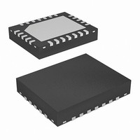
ISL8101IRZ Intersil, ISL8101IRZ Datasheet - Page 17

ISL8101IRZ
Manufacturer Part Number
ISL8101IRZ
Description
IC PWM CTRLR BUCK 2PHASE 24-QFN
Manufacturer
Intersil
Datasheet
1.ISL8101CRZ-T.pdf
(20 pages)
Specifications of ISL8101IRZ
Applications
Controller, Intel VRM9, VRM10, and AMD Hammer Applications
Voltage - Input
4.6 ~ 12 V
Number Of Outputs
1
Voltage - Output
0.6 ~ 2.3 V
Operating Temperature
-40°C ~ 85°C
Mounting Type
Surface Mount
Package / Case
24-VQFN Exposed Pad, 24-HVQFN, 24-SQFN, 24-DHVQFN
Lead Free Status / RoHS Status
Lead free / RoHS Compliant
close to the device. It is especially important to locate the
components associated with the feedback circuit close to
their respective controller pins, since they belong to a high-
impedance circuit loop, sensitive to EMI pick-up. It is
important to place the R
terminal of the ISL8101.
A multi-layer printed circuit board is recommended. Figure 10
shows the connections of the critical components for one
output channel of the converter. Note that capacitors C
and C
capacitors. Dedicate one solid layer, usually the one
underneath the component side of the board, for a ground
plane and make all critical component ground connections
with vias to this layer. Dedicate another solid layer as a power
plane and break this plane into smaller islands of common
voltage levels. Keep the metal runs from the PHASE terminal
to inductor L
+12V
+5V
R’
IN
R
IN
xxOUT
OFS
OFS
C
R
R
R
2
2
2
1
(MINIMIZE CONNECTION PATH)
OUT
could each represent numerous physical
DACSEL/VID12
R
LOCATE CLOSE TO IC
ISEN
short. The power plane should support the
(C
F1
SSEND
VRM10
C
COMP
)
ENLL
VID4
VID3
VID2
VID1
VID0
ISEN
1
OFS
FB
ISEN
17
resistor close to the respective
FIGURE 10. PRINTED CIRCUIT BOARD POWER PLANES AND ISLANDS
V
CC
ISL8101
P
VCC
(C
F2
)
xxIN
PHASE1
UGATE2
PHASE2
BOOT1
UGATE1
LGATE1
BOOT2
LGATE2
PGND
GND
L
IN
ISL8101
C
C
BOOT1
BOOT2
LOCATE NEAR SWITCHING TRANSISTORS;
input power and output power nodes. Use copper filled
polygons on the top and bottom circuit layers for the phase
nodes. Use the remaining printed circuit layers for small signal
wiring. The wiring traces from the IC to the MOSFETs’ gates
and sources should be sized to carry at least one ampere of
current (0.02” to 0.05”).
(MINIMIZE CONNECTION PATH)
Q
Q
Q
Q
3
4
1
2
(C
HFIN1
(C
KEY
HFIN2
L
L
)
HEAVY TRACE ON CIRCUIT PLANE LAYER
ISLAND ON POWER PLANE LAYER
ISLAND ON CIRCUIT PLANE LAYER
VIA CONNECTION TO GROUND PLANE
OUT1
OUT2
)
C
BIN2
C
BIN1
(MINIMIZE CONNECTION PATH)
LOCATE NEAR LOAD;
C
BOUT
(C
HFOUT
July 28, 2008
)
V
FN9223.1
OUT


