ISL8101IRZ Intersil, ISL8101IRZ Datasheet - Page 6
ISL8101IRZ
Manufacturer Part Number
ISL8101IRZ
Description
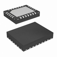
IC PWM CTRLR BUCK 2PHASE 24-QFN
Manufacturer
Intersil
Datasheet
1.ISL8101CRZ-T.pdf
(20 pages)
Specifications of ISL8101IRZ
Applications
Controller, Intel VRM9, VRM10, and AMD Hammer Applications
Voltage - Input
4.6 ~ 12 V
Number Of Outputs
1
Voltage - Output
0.6 ~ 2.3 V
Operating Temperature
-40°C ~ 85°C
Mounting Type
Surface Mount
Package / Case
24-VQFN Exposed Pad, 24-HVQFN, 24-SQFN, 24-DHVQFN
Lead Free Status / RoHS Status
Lead free / RoHS Compliant


referenced to the GND pin. LGATE drive is referenced to the
PGND pin.
VID0-4 (Pins 2, 1, 24-22)
Voltage identification inputs from microprocessor. These pins
respond to TTL logic thresholds. The ISL8101 decodes the
VID inputs to establish the output voltage; see VID Tables
beginning on page 9 for correspondence between DAC codes
and output voltage settings. These pins are internally pulled
high, to approximately 1.2V, by 40µA (typically) internal
current sources; the internal pull-up current decrease to 0 as
the VID voltage approaches the internal pull-up voltage. All
VID pins are compatible with external pull-up voltages not
exceeding the IC’s bias voltage.
DACSEL/VID5 (Pin 3)
If VRM10 pin is grounded, DACSEL/VID5 represents the 6th
voltage identification input from the VRM10-compliant
microprocessor, otherwise known as VID5. If VRM10 pin is
open or pulled high, DACSEL/VID5 selects the compliance
standard for the internal DAC: pulled to ground it encodes the
DAC with AMD Hammer VID codes, while left open or pulled
high, it encodes the DAC with Intel VRM9.0 codes.
VRM10 (Pin 4)
This pin selects VRM10.0 DAC compliance when grounded.
Left open, it allows selection of either VRM9.0 or Hammer
DAC compliance via DACSEL pin.
ENLL (Pin 21)
This pin is a precision-threshold (approximately 0.6V) enable
pin. Held low, this pin disables controller operation. Pulled
high, the pin enables the controller for operation.
FB and COMP (Pins 6, 5)
The internal error amplifier’s inverting input and output
respectively. These pins are connected to the external
network used to compensate the regulator’s feedback loop.
An internal current source injects the offset (OFS) current
sampled into the FB pin. Pulling COMP to ground through an
impedance lower than 15Ω disables the controller (same
effect as ENLL pulled low).
ISEN (Pin 7)
This pin is used to close the current-balance loop and set the
overcurrent protection threshold. A resistor connected
between this pin and V
equal to that sampled across the lower MOSFET’s r
during approximately the middle of its conduction interval.
The resulting current through this resistor is used for channel
current balancing and overcurrent protection. The voltage
across the R
two channels.
To select the proper R
R
ISEN
=
r
------------------------------------------------------ -
DS ON
ISEN
(
95μA
)MAX
resistor is time multiplexed between the
×
ISEN
CC
I
OUT
has a voltage drop forced across it
resistor, use Equation 1.
6
DS(ON)
(EQ. 1)
ISL8101
ISL8101
where:
r
resistance (Ω; include temperature effects)
I
See “Channel Balance Current Loop” on page 7 for more
information.
UGATE1, 2 (Pins 19, 12)
Connect these pins to the upper MOSFETs’ gates. These
pins are used to control the upper MOSFETs and are
monitored for shoot-through prevention purposes. Maximum
individual channel duty cycle is limited to 66%.
BOOT1, 2 (Pins 20, 11)
These pins provide the bias voltage for the upper MOSFETs’
drives. Connect these pins to appropriately-chosen external
bootstrap capacitors. Internal bootstrap diodes connected to
the PVCC pins provide the necessary bootstrap charge.
PHASE1, 2 (Pins 18, 13)
Connect these pins to the sources of the upper MOSFETs.
These pins are the return path for the upper MOSFETs’
drives.
LGATE1, 2 (Pins 17, 15)
These pins are used to control the lower MOSFETs and are
monitored for shoot-through prevention purposes. Connect
these pins to the lower MOSFETs’ gates.
OFS (Pin 9)
This pin is used to create an adjustable output voltage offset.
For no offset, leave this pin open. For negative offset, connect
a R’
Equation 2.
where:
V
For positive output voltage offset, connect a R
from this pin to GND, sizing it according to Equation 3.
For more information, refer to “Output Voltage Setting” on
page 9 .
SSEND (Pin 10)
This pin is an end of soft-start (SS) indicator; open drain
output device stays ON during soft-start, and goes open when
soft-start ends.
R′
R
OUT
DS(ON)MAX
OFFSET
OFS
OFS
OFS
= channel maximum output current (A)
=
=
resistor from this pin to V
R
R
= desired output voltage offset magnitude (mV)
1
1
×
×
= lower MOSFET’s highest drain-source ON
--------------------------
V
--------------------------
V
OFFSET
OFFSET
500
1500
CC
and size it according to
OFS
resistor
July 28, 2008
(EQ. 2)
(EQ. 3)
FN9223.1
Related parts for ISL8101IRZ
Image
Part Number
Description
Manufacturer
Datasheet
Request
R

Part Number:
Description:
Two-Phase Multiphase Buck PWM Controller
Manufacturer:
Intersil Corporation
Part Number:
Description:
Intersil Corporation [CMOS Serial Controller Interface]
Manufacturer:
Intersil Corporation
Datasheet:
Part Number:
Description:
Manufacturer:
Intersil Corporation
Datasheet:
Part Number:
Description:
357-036-542-201 CARDEDGE 36POS DL .156 BLK LOPRO
Manufacturer:
Intersil Corporation
Datasheet:
Part Number:
Description:
1024-Word x 4-Bit LSI Static RAM
Manufacturer:
Intersil Corporation
Datasheet:
Part Number:
Description:
General Purpose NPN Transistor Arrays FN341.4
Manufacturer:
Intersil Corporation
Datasheet:
Part Number:
Description:
CMOS 16-Bit Microprocessor
Manufacturer:
Intersil Corporation
Datasheet:
Part Number:
Description:
Manufacturer:
Intersil Corporation
Datasheet:
Part Number:
Description:
Manufacturer:
Intersil Corporation
Datasheet:
Part Number:
Description:
Manufacturer:
Intersil Corporation
Datasheet:
Part Number:
Description:
Manufacturer:
Intersil Corporation
Datasheet:
Part Number:
Description:
CMOS 6-Bit Latch and Decoder Memory Interfaces
Manufacturer:
Intersil Corporation
Datasheet:
Part Number:
Description:
CA3046General Purpose NPN Transistor Arrays
Manufacturer:
Intersil Corporation
Datasheet:
Part Number:
Description:
Manufacturer:
Intersil Corporation
Datasheet:
Part Number:
Description:
TR909 DLC/FLC SLIC with Low Power Standby
Manufacturer:
Intersil Corporation
Datasheet: