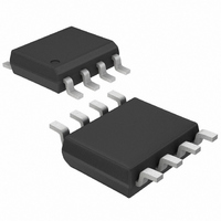
ICL7660ESA+ Maxim Integrated Products, ICL7660ESA+ Datasheet - Page 6

ICL7660ESA+
Manufacturer Part Number
ICL7660ESA+
Description
IC VOLTAGE CONVERTER 8-SOIC
Manufacturer
Maxim Integrated Products
Type
Switched Capacitor (Charge Pump), Divider, Doubler, Invertingr
Specifications of ICL7660ESA+
Internal Switch(s)
Yes
Synchronous Rectifier
No
Number Of Outputs
1
Current - Output
20mA
Frequency - Switching
10kHz
Voltage - Input
1.5 ~ 10 V
Operating Temperature
-40°C ~ 85°C
Mounting Type
Surface Mount
Package / Case
8-SOIC (3.9mm Width)
Power - Output
471mW
Function
Inverting/Step Up
Output Voltage
- 1.5 V to - 10 V or 3 V to 20 V
Output Current
20 mA
Maximum Operating Temperature
+ 85 C
Minimum Operating Temperature
- 40 C
Mounting Style
SMD/SMT
Primary Input Voltage
10V
No. Of Outputs
1
No. Of Pins
8
Operating Temperature Range
-40°C To +85°C
Dropout Voltage Vdo
500mV
Filter Terminals
SMD
Rohs Compliant
Yes
Lead Free Status / RoHS Status
Lead free / RoHS Compliant
Voltage - Output
-
Lead Free Status / Rohs Status
Lead free / RoHS Compliant
± 5V、1Gsps、8ビットADC
2.2GHzトラック/ホールドアンプ内蔵
Note 11: Effective Number of Bits (ENOB) are computed from a curve fit referenced to the theoretical full-scale range.
Note 12: Total Harmonic Distortion (THD) is computed from the first five harmonics.
Note 13: Guaranteed by design with a reset pulse one clock period long or greater.
Note 14: Guaranteed by design. The DREADY to DATA propagation delay is measured from the 50% point on the rising edge of the
標準動作特性 ______________________________________________________________________
(V
noted.)
6
CC
_______________________________________________________________________________________
8.00
7.75
7.50
7.25
7.00
6.75
6.50
A = V
55
50
45
40
35
30
10
10
(SINGLE-ENDED ANALOG INPUT DRIVE)
DREADY signal (when the output data changes) to the 50% point on a data output bit. This places the falling edge of the
DREADY signal in the middle of the data output valid window, within the differences between the DREADY and DATA rise
and fall times, which gives maximum setup and hold time for latching external data latches.
-12dB FS
-1dB FS
-6dB FS
CC
SIGNAL-TO-NOISE + DISTORTION
vs. ANALOG INPUT FREQUENCY
vs. ANALOG INPUT FREQUENCY
EFFECTIVE NUMBER OF BITS
I = V
ANALOG INPUT FREQUENCY (MHz)
ANALOG INPUT FREQUENCY (MHz)
DIFFERENTIAL ANALOG INPUT DRIVE
CC
100
D = +5V, V
100
1000
EE
-1dB FS
-6dB FS
-12dB FS
= -5V, V
1000
10,000
1250
CC
O = +3.3V, REFIN connected to REFOUT, f
8.00
7.75
7.50
7.25
7.00
6.75
6.50
50
46
42
38
34
30
10
10
(SINGLE-ENDED ANALOG INPUT DRIVE)
(DIFFERENTIAL ANALOG INPUT DRIVE)
vs. ANALOG INPUT FREQUENCY
vs. ANALOG INPUT FREQUENCY
EFFECTIVE NUMBER OF BITS
ANALOG INPUT FREQUENCY (MHz)
ANALOG INPUT FREQUENCY (MHz)
SIGNAL-TO-NOISE RATIO
100
100
-12dB FS
-1dB FS
-6dB FS
-12dB FS
-6dB FS
-1dB FS
1000
1000
1250
1250
S
= 1Gsps, T
55
50
45
40
35
30
50
46
42
38
34
30
10
10
-12dB FS
(DIFFERENTIAL ANALOG INPUT DRIVE)
-1dB FS
-6dB FS
SIGNAL-TO-NOISE + DISTORTION
A
vs. ANALOG INPUT FREQUENCY
vs. ANALOG INPUT FREQUENCY
ANALOG INPUT FREQUENCY (MHz)
= +25°C, unless otherwise
ANALOG INPUT FREQUENCY (MHz)
SINGLE-ENDED ANALOG INPUT DRIVE
SIGNAL-TO-NOISE RATIO
100
100
-12dB FS
-1dB FS
-6dB FS
1000
1000 1250
10,000


