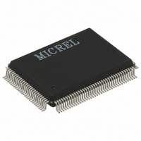
KS8995MA Micrel Inc, KS8995MA Datasheet - Page 12

KS8995MA
Manufacturer Part Number
KS8995MA
Description
IC SWITCH 10/100 5PORT 128PQFP
Manufacturer
Micrel Inc
Specifications of KS8995MA
Applications
*
Mounting Type
Surface Mount
Package / Case
128-MQFP, 128-PQFP
Number Of Primary Switch Ports
5
Internal Memory Buffer Size
64
Operating Supply Voltage (typ)
1.8/2.5/3.3V
Fiber Support
Yes
Integrated Led Drivers
Yes
Phy/transceiver Interface
MII/SNI
Power Supply Type
Analog/Digital
Package Type
PQFP
Data Rate (typ)
10/100Mbps
Vlan Support
Yes
Operating Temperature (max)
70C
Operating Temperature (min)
0C
Pin Count
128
Mounting
Surface Mount
Jtag Support
No
Operating Temperature Classification
Commercial
Data Rate
100Mbps
Lead Free Status / RoHS Status
Lead free / RoHS Compliant
For Use With
576-1017 - BOARD EVAL EXPERIMENT KS8995M
Lead Free Status / RoHS Status
Not Compliant, Lead free / RoHS Compliant
Available stocks
Company
Part Number
Manufacturer
Quantity
Price
Company:
Part Number:
KS8995MAI
Manufacturer:
MAXIM
Quantity:
4 430
Semptember 2008
Notes:
1.
Pin Number
P = Power supply.
I = Input.
O = Output.
I/O = Bidirectional.
Gnd = Ground.
Ipu = Input w/internal pull-up.
Ipd = Input w/internal pull-down.
Ipd/O = Input w/internal pull-down during reset, output pin otherwise.
Ipu/O = Input w/internal pull-up during reset, output pin otherwise.
NC = No connect.
31
32
33
34
35
36
37
38
39
40
41
42
43
44
45
46
47
48
49
50
51
52
53
54
55
56
57
58
59
60
FXSD5/FXSD3
PWRDN_N
RESERVE
Pin Name
PMTXEN
PMTXER
PMTXD3
PMTXD2
PMTXD1
PMTXD0
PMRXC
VDDAR
VDDAR
VDDAR
PMTXC
VDDAT
FXSD4
VDDIO
GNDA
GNDA
GNDA
GNDA
GNDD
GNDD
RXM5
MUX1
MUX2
VDDC
RXP5
TXM5
TXP5
Type
Gnd
Gnd
Gnd
Gnd
Gnd
Gnd
NC
Ipd
Ipd
NC
NC
Ipu
Ipd
Ipd
Ipd
Ipd
Ipd
Ipd
O
O
O
O
P
P
P
P
P
P
I
I
(1)
Port
5/3
5
5
5
5
4
5
5
5
5
5
5
5
5
Pin Function
1.8V analog V
Physical receive signal + (differential).
Physical receive signal – (differential).
Analog ground.
Physical transmit signal + (differential).
Physical transmit signal – (differential).
2.5V or 3.3V analog V
Fiber signal detect pin. FXSD5 is for port 5 of the KS8995MA. FXSD3
is for port 3 of the KS8995FQ
Fiber signal detect pin for port 4.
Analog ground.
1.8V analog V
Analog ground.
1.8V analog V
Analog ground.
Factory test pins. MUX1 and MUX2 should be left unconnected for
normal operation
Mode
Normal Operation
Full-chip power down. Active low.
Reserved pin. No connect.
Digital ground.
1.8V digital core V
PHY[5] MII transmit enable.
PHY[5] MII transmit bit 3.
PHY[5] MII transmit bit 2.
PHY[5] MII transmit bit 1.
PHY[5] MII transmit bit 0.
PHY[5] MII transmit error.
PHY[5] MII transmit clock. PHY mode MII.
Digital ground.
3.3V digital V
PHY[5] MII receive clock. PHY mode MII.
12
DD
DD
DD
DD
for digital I/O circuitry.
.
.
.
DD
.
DD
.
MUX1
NC
M9999-091508
MUX2
NC


