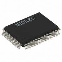
KS8995MA Micrel Inc, KS8995MA Datasheet - Page 43

KS8995MA
Manufacturer Part Number
KS8995MA
Description
IC SWITCH 10/100 5PORT 128PQFP
Manufacturer
Micrel Inc
Specifications of KS8995MA
Applications
*
Mounting Type
Surface Mount
Package / Case
128-MQFP, 128-PQFP
Number Of Primary Switch Ports
5
Internal Memory Buffer Size
64
Operating Supply Voltage (typ)
1.8/2.5/3.3V
Fiber Support
Yes
Integrated Led Drivers
Yes
Phy/transceiver Interface
MII/SNI
Power Supply Type
Analog/Digital
Package Type
PQFP
Data Rate (typ)
10/100Mbps
Vlan Support
Yes
Operating Temperature (max)
70C
Operating Temperature (min)
0C
Pin Count
128
Mounting
Surface Mount
Jtag Support
No
Operating Temperature Classification
Commercial
Data Rate
100Mbps
Lead Free Status / RoHS Status
Lead free / RoHS Compliant
For Use With
576-1017 - BOARD EVAL EXPERIMENT KS8995M
Lead Free Status / RoHS Status
Not Compliant, Lead free / RoHS Compliant
Available stocks
Company
Part Number
Manufacturer
Quantity
Price
Company:
Part Number:
KS8995MAI
Manufacturer:
MAXIM
Quantity:
4 430
Semptember 2008
Global Registers
Address
Register 0 (0x00): Chip ID0
7-0
Register 1 (0x01): Chip ID1 / Start Switch
7-4
3-1
0
Register 2 (0x02): Global Control 0
7
6-4
3
2
1
0
Register 3 (0x03): Global Control 1
7
6
Name
family ID
Chip ID
Revision ID
Start Switch
Reserved
802.1p Base Priority
Enable PHY MII
Buffer Share Mode
UNH Mode
Link Change Age
Pass All Frames
Reserved
Description
Chip family.
0x0 is assigned to M series. (95MA)
Revision ID
1, start the chip when external pins (PS1, PS0) = (1,0) or
(0,1). Note: in (PS1,PS0) = (0,0) mode, the chip will
start automatically, after trying to read the external
EEPROM. If EEPROM does not exist, the chip will use
default values for all internal registers. If EEPROM is
present, the contents in the EEPROM will be checked.
The switch will check: (1) Register 0 = 0x95,
(2) Register 1 [7:4] = 0x0. If this check is OK, the
contents in the EEPROM will override chip register
default values =0, chip will not start when external pins
(PS1, PS0) = (1,0) or (0,1).
Note: (PS1, PS0) = (1,1) for Factory test only.
Reserved.
Used to classify priority for incoming 802.1q packets
“User priority” is compared against this value ⊕ :
classified as high priority. < : classified as low priority.
1, enable PHY MII-P5 interface.
Note: if not enabled, the switch will tri-state all outputs.
1, buffer pool is shared by all ports. A port can use more
buffer when other ports are not busy.
0, a port is only allowed to use 1/5 of the buffer pool.
1, the switch will drop packets with 0x8808 in T/L filed, or
DA=01-80-C2-00-00-01.
0, the switch will drop packets qualified as “flow control”
packets.
1, link change from “link” to “no link” will cause fast aging
(<800µs) to age address table faster. After an age cycle
is complete, the age logic will return to normal (300 + 75
seconds ). Note: If any port is
unplugged, all addresses will be automatically aged out.
1, switch all packets including bad ones. Used solely for
debugging purpose. Works in conjunction with
sniffer mode.
Reserved.
43
Mode
R/W
R/W
R/W
R/W
R/W
R/W
R/W
R/W
RW
RO
RO
RO
Based on real chip
revision. 0x02=B2,
0x03=B3,
0x04=B4,
0x05=B5, etc.
Pin LED5-1 strap
option.
Pull-down (0):
isolate. Pull-up
(1): Enable.
Note: LED[5][1]
has internal pull-
up.
M9999-091508
Default
0x95
0x0
0x0
0x0
0x4
0x1
0
0
0
0


