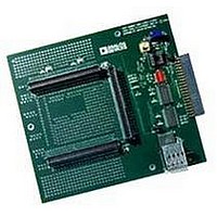
ADZS-21262-1-EZEXT Analog Devices Inc, ADZS-21262-1-EZEXT Datasheet - Page 38

ADZS-21262-1-EZEXT
Manufacturer Part Number
ADZS-21262-1-EZEXT
Description
BOARD DAUGHTER FOR ADSP-21262
Manufacturer
Analog Devices Inc
Datasheet
1.ADSP-21363KSWZ-1AA.pdf
(56 pages)
Specifications of ADZS-21262-1-EZEXT
Accessory Type
DSP
Silicon Manufacturer
Analog Devices
Core Architecture
SHARC
Features
Expansion Interface, High Speed Converter (HSC) Interface
Kit Contents
Board Docs
Silicon Family Name
SHARC
Silicon Core Number
ADSP-21262
Rohs Compliant
Yes
Lead Free Status / RoHS Status
Lead free / RoHS Compliant
For Use With/related Products
ADSP-21262
Lead Free Status / RoHS Status
Lead free / RoHS Compliant, Lead free / RoHS Compliant
ADSP-21362/ADSP-21363/ADSP-21364/ADSP-21365/ADSP-21366
S/PDIF Transmitter Input Data Timing
The timing requirements for the S/PDIF transmitter are given
in
using the SRU. Therefore, the timing specifications provided
below are valid at the DAI_P20–1 pins.
Table 36. S/PDIF Transmitter Input Data Timing
1
Oversampling Clock (TxCLK) Switching Characteristics
The S/PDIF transmitter requires an oversampling clock input.
This high frequency clock (TxCLK) input is divided down to
generate the internal biphase clock.
Table 37. Oversampling Clock (TxCLK) Switching Characteristics
Parameter
Timing Requirements
t
t
t
t
t
t
t
t
Parameter
Frequency for TxCLK = 384 × Frame Sync
Frequency for TxCLK = 256 × Frame Sync
Frame Rate (FS)
The serial clock, data and frame sync signals can come from any of the DAI pins.The serial clock and frame sync signals can also come via PCG or SPORTs. PCG’s input can
SISFS
SIHFS
SISD
SIHD
SITXCLKW
SITXCLK
SISCLKW
SISCLK
be either CLKIN or any of the DAI pins.
Table
1
1
1
1
36. Input signals are routed to the DAI_P20–1 pins
Frame Sync Setup Before Serial Clock Rising Edge
Frame Sync Hold After Serial Clock Rising Edge
Data Setup Before Serial Clock Rising Edge
Data Hold After Serial Clock Rising Edge
Transmit Clock Width
Transmit Clock Period
Clock Width
Clock Period
DAI_P20–1
DAI_P20–1
DAI_P20–1
DAI_P20–1
(SDATA)
(TxCLK)
(SCLK)
(FS)
t
SITXCLKW
Figure 32. S/PDIF Transmitter Input Timing
Rev. G | Page 38 of 56 | March 2011
t
SISCLKW
SAMPLE EDGE
t
SISFS
t
SISD
t
SISCLK
t
SITXCLK
Min
3
3
3
3
9
20
36
80
Max
Oversampling Ratio × Frame Sync <= 1/t
49.2
192.0
K Grade
t
t
SIHFS
SIHD
Max
Min
3
3
3
3
9.5
20
36
80
Y Grade
Max
SITXCLK
Unit
MHz
MHz
kHz
Unit
ns
ns
ns
ns
ns
ns
ns
ns


