MCP1631RD-MCC2 Microchip Technology, MCP1631RD-MCC2 Datasheet - Page 109
MCP1631RD-MCC2
Manufacturer Part Number
MCP1631RD-MCC2
Description
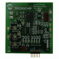
REFERENCE DESIGN MCP1631HV
Manufacturer
Microchip Technology
Datasheets
1.MCP1631VHVT-330EST.pdf
(34 pages)
2.MCP1631HV-330EST.pdf
(54 pages)
3.MCP1631RD-MCC2.pdf
(20 pages)
4.MCP1631RD-MCC2.pdf
(328 pages)
Specifications of MCP1631RD-MCC2
Main Purpose
Power Management, Battery Charger
Embedded
Yes, MCU, 8-Bit
Utilized Ic / Part
MCP1631HV, PIC16F883
Primary Attributes
1 ~ 2 Cell- Li-Ion, 1 ~ 5 Cell- NiCd/NiMH, 1 ~ 2 1W LEDs
Secondary Attributes
Status LEDs
Silicon Manufacturer
Microchip
Application Sub Type
Battery Charger
Kit Application Type
Power Management - Battery
Silicon Core Number
MCP1631HV, PIC16F883
Kit Contents
Board
Lead Free Status / RoHS Status
Lead free / RoHS Compliant
Lead Free Status / RoHS Status
Lead free / RoHS Compliant


9.3
For the ADC to meet its specified accuracy, the charge
holding capacitor (C
charge to the input channel voltage level. The Analog
Input model is shown in Figure 9-4. The source
impedance (R
impedance directly affect the time required to charge the
capacitor C
varies over the device voltage (V
The maximum recommended impedance for analog
sources is 10 kΩ. As the source impedance is
decreased, the acquisition time may be decreased.
After the analog input channel is selected (or changed),
EQUATION 9-1:
© 2009 Microchip Technology Inc.
Note 1: The reference voltage (V
The value for T
Solving for T
Therefore:
Assumptions:
V
V
V
2: The charge holding capacitor (C
3: The maximum recommended impedance for analog sources is 10 kΩ. This is required to meet the pin
A/D Acquisition Requirements
AP PLIE D
AP P LI ED
AP P LIED
HOLD
T
leakage specification.
S
ACQ
T
) and the internal sampling switch (R
T
. The sampling switch (R
ACQ
C
⎛
⎝
C
⎛
⎜
⎝
⎛
⎜
⎝
=
=
=
1
=
=
:
1 e
1 e
C
HOLD
=
=
=
–
2
ACQUISITION TIME EXAMPLE
Temperature
–
–
4.67
–
can be approximated with the following equations:
–
1.37
ΜS
10pF 1k
--------------------------
(
C
Amplifier Settling Time
T
2µs
2
) must be allowed to fully
AMP
HOLD
–
--------- -
–
-------- -
RC
+
n
RC
ΜS
µs
T
Tc
+
+
C
1.37
(
1
⎞
⎟
⎠
⎞
⎟
⎠
1
+
T
(
) 1
R
C
=
=
Ω
T
ΜS
DD
–
IC
+
C
+
), see Figure 9-4.
V
V
+
+
[
+
REF
⎞
⎠
(
7k
=
CHOLD
A P PLIE D
Temperature - 25°C
T
R
[
SS
(
Ω
COFF
=
) has no effect on the equation, since it cancels itself out.
SS
50°C- 25°C
) impedance
50°C and external impedance of 10k
+
+
V
HOLD
10k
CHOLD
R
PIC16F882/883/884/886/887
S
⎛
⎝
) ln(1/2047)
+
1
Ω
) is not discharged after each conversion.
SS
)
Hold Capacitor Charging Time
–
ln(0.0004885)
)
) 0.05
--------------------------
(
(
2
n
+
) 0.05µs/°C
1
ΜS
1
(
) 1
/°C
an A/D acquisition must be done before the conversion
can be started. To calculate the minimum acquisition
time, Equation 9-1 may be used. This equation
assumes that 1/2 LSb error is used (1024 steps for the
ADC). The 1/2 LSb error is the maximum error allowed
for the ADC to meet its specified resolution.
–
)
⎞
⎠
]
;[2] V
;combining [1] and [2]
;[1] V
)
]
CHOLD
CHOLD
Ω
5.0V V
+
charge response to V
charged to within 1/2 lsb
Temperature Coefficient
DD
DS41291F-page 107
APPLIED
Related parts for MCP1631RD-MCC2
Image
Part Number
Description
Manufacturer
Datasheet
Request
R

Part Number:
Description:
REFERENCE DESIGN FOR MCP1631HV
Manufacturer:
Microchip Technology
Datasheet:

Part Number:
Description:
REF DES BATT CHARG OR LED DRIVER
Manufacturer:
Microchip Technology
Datasheet:

Part Number:
Description:
Manufacturer:
Microchip Technology Inc.
Datasheet:
Part Number:
Description:
Manufacturer:
Microchip Technology Inc.
Datasheet:
Part Number:
Description:
Manufacturer:
Microchip Technology Inc.
Datasheet:
Part Number:
Description:
Manufacturer:
Microchip Technology Inc.
Datasheet:
Part Number:
Description:
Manufacturer:
Microchip Technology Inc.
Datasheet:
Part Number:
Description:
Manufacturer:
Microchip Technology Inc.
Datasheet:
Part Number:
Description:
Manufacturer:
Microchip Technology Inc.
Datasheet:
Part Number:
Description:
Manufacturer:
Microchip Technology Inc.
Datasheet: