MCP1631RD-MCC2 Microchip Technology, MCP1631RD-MCC2 Datasheet - Page 95
MCP1631RD-MCC2
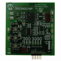
Manufacturer Part Number
MCP1631RD-MCC2
Description
REFERENCE DESIGN MCP1631HV
Manufacturer
Microchip Technology
Datasheets
1.MCP1631VHVT-330EST.pdf
(34 pages)
2.MCP1631HV-330EST.pdf
(54 pages)
3.MCP1631RD-MCC2.pdf
(20 pages)
4.MCP1631RD-MCC2.pdf
(328 pages)
Specifications of MCP1631RD-MCC2
Main Purpose
Power Management, Battery Charger
Embedded
Yes, MCU, 8-Bit
Utilized Ic / Part
MCP1631HV, PIC16F883
Primary Attributes
1 ~ 2 Cell- Li-Ion, 1 ~ 5 Cell- NiCd/NiMH, 1 ~ 2 1W LEDs
Secondary Attributes
Status LEDs
Silicon Manufacturer
Microchip
Application Sub Type
Battery Charger
Kit Application Type
Power Management - Battery
Silicon Core Number
MCP1631HV, PIC16F883
Kit Contents
Board
Lead Free Status / RoHS Status
Lead free / RoHS Compliant
Lead Free Status / RoHS Status
Lead free / RoHS Compliant


REGISTER 8-4:
© 2009 Microchip Technology Inc.
bit 7
Legend:
R = Readable bit
-n = Value at POR
bit 7
bit 6
bit 5
bit 4
bit 3
bit 2
bit 1
bit 0
Note 1:
R/W-0
SR1
2:
(2)
The CxOUT bit in the CMxCON0 register will always reflect the actual comparator output (not the level on
the pin), regardless of the SR latch operation.
To enable an SR Latch output to the pin, the appropriate CxOE and TRIS bits must be properly
configured.
SR1: SR Latch Configuration bit
1 =
0 =
SR0: SR Latch Configuration bits
1 =
0 =
C1SEN: C1 Set Enable bit
1 = C1 comparator output sets SR latch
0 = C1 comparator output has no effect on SR latch
C2REN: C2 Reset Enable bit
1 = C2 comparator output resets SR latch
0 = C2 comparator output has no effect on SR latch
PULSS: Pulse the SET Input of the SR Latch bit
1 = Triggers pulse generator to set SR latch. Bit is immediately reset by hardware.
0 = Does not trigger pulse generator
PULSR: Pulse the Reset Input of the SR Latch bit
1 = Triggers pulse generator to reset SR latch. Bit is immediately reset by hardware.
0 = Does not trigger pulse generator
Unimplemented: Read as ‘0’
FVREN: Fixed Voltage Reference Enable bit
1 = 0.6V Reference FROM INTOSC LDO is enabled
0 = 0.6V Reference FROM INTOSC LDO is disabled
SR0
R/W-0
C2OUT pin is the latch Q output
C2OUT pin is the C2 comparator output
C1OUT pin is the latch Q output
C1OUT pin is the C1 Comparator output
SRCON: SR LATCH CONTROL REGISTER
(2)
W = Writable bit
‘1’ = Bit is set
C1SEN
R/W-0
PIC16F882/883/884/886/887
C2REN
(2)
R/W-0
(2)
S = Bit is set only -
U = Unimplemented bit, read as ‘0’
‘0’ = Bit is cleared
PULSS
R/S-0
PULSR
R/S-0
x = Bit is unknown
U-0
—
DS41291F-page 93
FVREN
R/W-0
bit 0
Related parts for MCP1631RD-MCC2
Image
Part Number
Description
Manufacturer
Datasheet
Request
R

Part Number:
Description:
REFERENCE DESIGN FOR MCP1631HV
Manufacturer:
Microchip Technology
Datasheet:

Part Number:
Description:
REF DES BATT CHARG OR LED DRIVER
Manufacturer:
Microchip Technology
Datasheet:

Part Number:
Description:
Manufacturer:
Microchip Technology Inc.
Datasheet:
Part Number:
Description:
Manufacturer:
Microchip Technology Inc.
Datasheet:
Part Number:
Description:
Manufacturer:
Microchip Technology Inc.
Datasheet:
Part Number:
Description:
Manufacturer:
Microchip Technology Inc.
Datasheet:
Part Number:
Description:
Manufacturer:
Microchip Technology Inc.
Datasheet:
Part Number:
Description:
Manufacturer:
Microchip Technology Inc.
Datasheet:
Part Number:
Description:
Manufacturer:
Microchip Technology Inc.
Datasheet:
Part Number:
Description:
Manufacturer:
Microchip Technology Inc.
Datasheet: