STEVAL-IPE009V1 STMicroelectronics, STEVAL-IPE009V1 Datasheet - Page 30
STEVAL-IPE009V1
Manufacturer Part Number
STEVAL-IPE009V1
Description
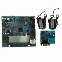
BOARD EVAL ST72321BR9/STPM14
Manufacturer
STMicroelectronics
Type
Other Power Managementr
Specifications of STEVAL-IPE009V1
Main Purpose
Power Management, Energy/Power Meter
Embedded
Yes, MCU, 8-Bit
Utilized Ic / Part
STPM14, ST72F321BR9T6
Primary Attributes
1-Ph 220 VAC, LCD Displays: No-Load, Reverse, Fraud, or Case Tampering
Secondary Attributes
Up to 4 Tariff Rates, Data Accumulated for Meter Life, Time Stamp for: Tamper, Fraud, Power Failure
Input Voltage
220 V
Product
Power Management Modules
Silicon Manufacturer
ST Micro
Silicon Core Number
ST72321BR9 And STPM14
Features
Continuously Detects, Displays No-Load Condition, Reverse Direction, Fraud And Case Tamper Condition
Lead Free Status / RoHS Status
Lead free / RoHS Compliant
For Use With/related Products
STPM14, ST72321BR9
Other names
497-8434
STEVAL-IPE009V1
STEVAL-IPE009V1


Theory of operation
7.16
Table 16.
7.17
30/46
Signal
PUMP
Name
WE
RD
Value
Mode signals
The STPM1x includes four mode signals. These signals change some of the operation of
the STPM1x. The mode signals are not retained when the STPM1x supply is not available
and then they are cleared when a POR occurs.
The mode signals bit can be written using the normal writing procedure of the CFGI
interface (see CFGI par. 7.17)
Mode signals description
CFGI: configuration interface
The CFGI interface supports a simple serial protocol, which is implemented in order to
enable the configuration of STPM1x which allows writing the mode bits and the
configuration bits (temporarily or permanently);
Four pins of the device are dedicated to this purpose: SCS, SYN-NP, SCLNCN, SDATD.
SCS, SYN-NP, SCL-NLC and SDATD are all input pins. A high level signal for these pins
means a voltage level higher than 0.75 x V
lower than 0.25 x V
Bit
0
1
0
1
0
1
– RD mode signal has been already described in par.
– PUMP. When set, the PUMP mode signal transforms the MOP and MON pins to act
– WE (write Enable): This mode signal is used to permanently write to the OTP anti-
but there is another implied function of the signal RD. When it is set, each sense
amplifier is disconnected from corresponding antifuse element and this way, its 3 V
NMOS gate is protected from the high voltage of V
operation. This means that as long as the V
signal RD should be set.
as driving signals to implement a charge-pump DC-DC converter (see
This feature is useful in order to boost the V
generate the V
elements.
fuse element. When this bit is not set, any writing to the configuration bit is recorded
in the shadow latches. When this bit is set, the writing is recorded both in the shadow
latch and in the OTP anti-fuse element.
MOP and MON operate normally
MOP and MON provide the driving signals to implement a
charge-pump DC-DC converter
The 56 Configuration bits originated by OTP anti-fuses
The 56 Configuration bits originated by shadow latches
Any writing in the configuration bits is recorded in the shadow
latches
Any writing in the configuration bits is recorded both in the
shadow latches and in the OTP anti-fuse elements
CC
OTP
.
voltage (14 V to 20 V) needed to program the OTP anti-fuse
Doc ID 13167 Rev 7
Status
CC
, while a low level signal means a voltage value
OTP
CC
STPM11, STPM12, STPM13, STPM14
supply voltage of the STPM1x to
voltage reads more than 3 V, the
OTP
7.15
during permanent write
(configuring the STPM1x),
Command
1111101x
0111001x
1111001x
0111101x
0111110x
1111110x
Binary
Figure
Command
FC or FD
7C or 7D
7A or 7B
FA or FB
F2 or F3
72 or 73
Hex
23).
Related parts for STEVAL-IPE009V1
Image
Part Number
Description
Manufacturer
Datasheet
Request
R

Part Number:
Description:
BOARD DEMO TFT DISPLAY STR91
Manufacturer:
STMicroelectronics
Datasheet:

Part Number:
Description:
BOARD EVAL FOR MEMS SENSORS
Manufacturer:
STMicroelectronics
Datasheet:

Part Number:
Description:
KIT DEV STARTER ST10F276Z5
Manufacturer:
STMicroelectronics
Datasheet:

Part Number:
Description:
BOARD EVAL HDMI $ VIDEO SWITCH
Manufacturer:
STMicroelectronics
Datasheet:

Part Number:
Description:
BOARD DEMO ACCELEROMETER DIL24
Manufacturer:
STMicroelectronics
Datasheet:

Part Number:
Description:
BOARD STLM75/STDS75/ST72F651
Manufacturer:
STMicroelectronics
Datasheet:

Part Number:
Description:
EVAL BOARD 3AXIS MEMS ACCELLRMTR
Manufacturer:
STMicroelectronics
Datasheet:

Part Number:
Description:
BOARD EVAL 8BIT MICRO + TDE1708
Manufacturer:
STMicroelectronics
Datasheet:

Part Number:
Description:
EVAL BOARD A/D TS4657
Manufacturer:
STMicroelectronics
Datasheet:

Part Number:
Description:
BOARD ADAPTER 20DIP LIS3LV02DL
Manufacturer:
STMicroelectronics
Datasheet:
Part Number:
Description:
STMicroelectronics [RIPPLE-CARRY BINARY COUNTER/DIVIDERS]
Manufacturer:
STMicroelectronics
Datasheet:
Part Number:
Description:
STMicroelectronics [LIQUID-CRYSTAL DISPLAY DRIVERS]
Manufacturer:
STMicroelectronics
Datasheet:
Part Number:
Description:
BOARD EVAL FOR MEMS SENSORS
Manufacturer:
STMicroelectronics
Datasheet: