DC-VIDEO-TVP5146N Altera, DC-VIDEO-TVP5146N Datasheet - Page 14
DC-VIDEO-TVP5146N
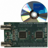
Manufacturer Part Number
DC-VIDEO-TVP5146N
Description
VIDEO DAUGHTER CARD
Manufacturer
Altera
Series
Stratix® IIIr
Datasheets
1.EP3SL150F780C4N.pdf
(16 pages)
2.EP3SL150F780C4N.pdf
(332 pages)
3.DC-VIDEO-TVP5146N.pdf
(58 pages)
Specifications of DC-VIDEO-TVP5146N
Main Purpose
Video, Daughter Card
Embedded
No
Utilized Ic / Part
Altera Dev Kits
Primary Attributes
Dual Composite Video Input - NTSC or PAL
Secondary Attributes
10-bit BT.656 Output, Compatible with Expansion Connector, Standard on Most Altera Development Kits
Lead Free Status / RoHS Status
Lead free / RoHS Compliant
Other names
544-1704


Table 1–20. PLL Specifications for Stratix III Devices (Part 1 of 3)
f
f
f
t
f
f
t
t
t
t
f
t
t
IN
INPFD
VCO
EINDUTY
OUT
OUT_EXT
OUTDUTY
FCOMP
CONFIGPLL
CONFIGPHASE
SCANCLK
LOCK
DLOCK
Symbol
Input clock frequency
Input frequency to the PFD
PLL VCO operating range
Input clock or external feedback
clock input duty cycle
Output frequency for internal global
or regional clock
Output frequency for dedicated
external clock output
Duty cycle for external clock output
(when set to 50%)
External feedback clock
compensation time
Time required to reconfigure scan
chain
Time required to reconfigure phase
shift
scanclk frequency
Time required to lock from end of
device configuration
Time required to lock dynamically
(after switchover or reconfiguring
any non-post-scale
counters/delays)
Parameter
Min
600
40
—
—
45
—
—
—
—
—
—
5
5
V
CCL
Typ
= 1.1 V
3.5
C2
—
—
—
—
—
—
50
—
—
—
—
1
1600
Max
800
325
600
800
100
(1)
(2)
(2)
60
55
10
—
—
1
1
Min
600
40
—
—
45
—
—
—
—
—
—
5
5
V
CCL
C3, I3
Typ
3.5
= 1.1 V
—
—
—
—
—
—
50
—
—
—
—
1
1300
Max
717
325
500
717
100
(1)
(2)
(2)
60
55
10
—
—
1
1
Min
600
40
—
—
45
—
—
—
—
—
—
5
5
V
CCL
C4, I4
Typ
= 1.1 V
3.5
—
—
—
—
—
—
50
—
—
—
—
1
1300
Max
717
325
450
717
100
(1)
(2)
(2)
60
55
10
—
—
1
1
Min
600
40
—
—
45
—
—
—
—
—
—
5
5
V
CCL
Typ
3.5
= 1.1 V
—
—
—
—
—
—
50
—
—
—
—
1
1300
Max
717
325
450
717
100
(1)
(2)
(2)
60
55
10
—
—
C4L, I4L
1
1
Min
600
40
—
—
45
—
—
—
—
—
—
5
5
V
CCL
Typ
= 0.9 V
3.5
—
—
—
—
—
—
50
—
—
—
—
1
1300
Max
717
325
375
717
100
(1)
60
(2)
(2)
55
10
—
—
1
1
scanclk
scanclk
cycles
cycles
Unit
MHz
MHz
MHz
MHz
MHz
MHz
ms
ms
ns
%
%
Related parts for DC-VIDEO-TVP5146N
Image
Part Number
Description
Manufacturer
Datasheet
Request
R

Part Number:
Description:
CYCLONE II STARTER KIT EP2C20N
Manufacturer:
Altera
Datasheet:


Part Number:
Description:
CPLD, EP610 Family, ECMOS Process, 300 Gates, 16 Macro Cells, 16 Reg., 16 User I/Os, 5V Supply, 35 Speed Grade, 24DIP
Manufacturer:
Altera Corporation
Datasheet:
Part Number:
Description:
CPLD, EP610 Family, ECMOS Process, 300 Gates, 16 Macro Cells, 16 Reg., 16 User I/Os, 5V Supply, 15 Speed Grade, 24DIP
Manufacturer:
Altera Corporation
Datasheet:
Part Number:
Description:
Manufacturer:
Altera Corporation
Datasheet:
Part Number:
Description:
CPLD, EP610 Family, ECMOS Process, 300 Gates, 16 Macro Cells, 16 Reg., 16 User I/Os, 5V Supply, 30 Speed Grade, 24DIP
Manufacturer:
Altera Corporation
Datasheet:
Part Number:
Description:
High-performance, low-power erasable programmable logic devices with 8 macrocells, 10ns
Manufacturer:
Altera Corporation
Datasheet:
Part Number:
Description:
High-performance, low-power erasable programmable logic devices with 8 macrocells, 7ns
Manufacturer:
Altera Corporation
Datasheet:
Part Number:
Description:
Classic EPLD
Manufacturer:
Altera Corporation
Datasheet:
Part Number:
Description:
High-performance, low-power erasable programmable logic devices with 8 macrocells, 10ns
Manufacturer:
Altera Corporation
Datasheet:
Part Number:
Description:
Manufacturer:
Altera Corporation
Datasheet:
Part Number:
Description:
Manufacturer:
Altera Corporation
Datasheet:
Part Number:
Description:
Manufacturer:
Altera Corporation
Datasheet:
Part Number:
Description:
CPLD, EP610 Family, ECMOS Process, 300 Gates, 16 Macro Cells, 16 Reg., 16 User I/Os, 5V Supply, 25 Speed Grade, 24DIP
Manufacturer:
Altera Corporation
Datasheet: