DC-VIDEO-TVP5146N Altera, DC-VIDEO-TVP5146N Datasheet - Page 38
DC-VIDEO-TVP5146N
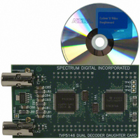
Manufacturer Part Number
DC-VIDEO-TVP5146N
Description
VIDEO DAUGHTER CARD
Manufacturer
Altera
Series
Stratix® IIIr
Datasheets
1.EP3SL150F780C4N.pdf
(16 pages)
2.EP3SL150F780C4N.pdf
(332 pages)
3.DC-VIDEO-TVP5146N.pdf
(58 pages)
Specifications of DC-VIDEO-TVP5146N
Main Purpose
Video, Daughter Card
Embedded
No
Utilized Ic / Part
Altera Dev Kits
Primary Attributes
Dual Composite Video Input - NTSC or PAL
Secondary Attributes
10-bit BT.656 Output, Compatible with Expansion Connector, Standard on Most Altera Development Kits
Lead Free Status / RoHS Status
Lead free / RoHS Compliant
Other names
544-1704


1–38
Programmable Output Buffer Delay
User I/O Pin Timing
Table 1–41. EP3SL50 Column Pins Input Timing Parameters (Part 1 of 3)
Stratix III Device Handbook, Volume 2
3.3-V
LVTTL
3.3-V
LVCMOS
3.0-V
LVTTL
Standard
I/O
Clock
GCLK
GCLK
GCLK
GCLK
GCLK
GCLK
PLL
PLL
PLL
t
t
t
t
t
t
t
t
t
t
t
t
su
su
su
su
su
su
h
h
h
h
h
h
Table 1–40
of the output buffer. The default delay is 0 ps.
Table 1–40. Programmable Output Buffer Delay
Table 1–41
buffer t
non-PLL global clock (GCLK) and the PLL is driven by the global clock (GCLK-PLL).
For t
for each device to the GCLK/GCLK-PLL values for the device.
EP3SL50 I/O Timing Parameters
Table 1–41
devices for single-ended I/O standards.
Table 1–41
I/O standards.
D
Note to
(1) You can set the programmable output buffer delay in the Quartus II software by setting the Output Buffer Delay
OUTBUF
Industrial
-0.690
-0.975
-0.690
-0.975
-0.701
-0.986
Control assignment to either positive, negative, or both edges with the specific values stated in this table for the
Output Buffer Delay assignment.
0.816
1.226
0.816
1.226
0.827
1.237
su
, t
Table
su
Symbol
h
Fast Model
, t
, and t
h
lists the delay chain settings that control the rising and falling edge delays
through
through
lists the EP3SL50 column pins input timing parameters for single-ended
, and t
1–40:
Commercial
-0.689
-0.975
-0.689
-0.975
-0.700
-0.986
co
0.814
1.226
0.814
1.226
0.825
1.237
using the regional clock, add the value from the adder tables listed
co
are reported for the cases when the I/O clock is driven by a
Table 1–140
Table 1–44
Rising and/or Falling
Edge delay
-1.004 -1.103 -1.311 -1.266 -1.627 -1.103 -1.311 -1.266 -1.627
-1.405 -1.532 -1.773 -1.713 -2.026 -1.532 -1.773 -1.713 -2.026
-1.004 -1.103 -1.311 -1.266 -1.627 -1.103 -1.311 -1.266 -1.627
-1.405 -1.532 -1.773 -1.713 -2.026 -1.532 -1.773 -1.713 -2.026
-1.003 -1.105 -1.310 -1.265 -1.626 -1.105 -1.310 -1.265 -1.626
-1.404 -1.534 -1.772 -1.712 -2.025 -1.534 -1.772 -1.712 -2.025
1.182
1.774
1.182
1.774
1.181
1.773
1.1 V
V
C2
CCL
Parameter
=
list the maximum I/O timing parameters for EP3SL50
Chapter 1: Stratix III Device Datasheet: DC and Switching Characteristics
list user I/O pin timing for Stratix III devices. I/O
1.304
1.947
1.304
1.947
1.306
1.949
1.1 V
V
C3
CCL
=
1.531
2.232
1.531
2.232
1.530
2.231
1.1 V
V
C4
CCL
(Note 1)
=
1.475
2.148
1.475
2.148
1.474
2.147
1.1 V
V
CCL
0 (default)
Typical
=
C4L
100
150
50
1.830
2.471
1.830
2.471
1.829
2.470
0.9 V
V
CCL
=
© July 2010 Altera Corporation
1.304
1.947
1.304
1.947
1.306
1.949
1.1 V
V
I3
CCL
=
1.531
2.232
1.531
2.232
1.530
2.231
1.1 V
V
I4
CCL
=
Unit
ps
ps
ps
ps
1.475
2.148
1.475
2.148
1.474
2.147
1.1 V
V
I/O Timing
CCL
=
I4L
1.830
2.471
1.830
2.471
1.829
2.470
0.9 V
V
CCL
=
Units
ns
ns
ns
ns
ns
ns
ns
ns
ns
ns
ns
ns
Related parts for DC-VIDEO-TVP5146N
Image
Part Number
Description
Manufacturer
Datasheet
Request
R

Part Number:
Description:
CYCLONE II STARTER KIT EP2C20N
Manufacturer:
Altera
Datasheet:


Part Number:
Description:
CPLD, EP610 Family, ECMOS Process, 300 Gates, 16 Macro Cells, 16 Reg., 16 User I/Os, 5V Supply, 35 Speed Grade, 24DIP
Manufacturer:
Altera Corporation
Datasheet:
Part Number:
Description:
CPLD, EP610 Family, ECMOS Process, 300 Gates, 16 Macro Cells, 16 Reg., 16 User I/Os, 5V Supply, 15 Speed Grade, 24DIP
Manufacturer:
Altera Corporation
Datasheet:
Part Number:
Description:
Manufacturer:
Altera Corporation
Datasheet:
Part Number:
Description:
CPLD, EP610 Family, ECMOS Process, 300 Gates, 16 Macro Cells, 16 Reg., 16 User I/Os, 5V Supply, 30 Speed Grade, 24DIP
Manufacturer:
Altera Corporation
Datasheet:
Part Number:
Description:
High-performance, low-power erasable programmable logic devices with 8 macrocells, 10ns
Manufacturer:
Altera Corporation
Datasheet:
Part Number:
Description:
High-performance, low-power erasable programmable logic devices with 8 macrocells, 7ns
Manufacturer:
Altera Corporation
Datasheet:
Part Number:
Description:
Classic EPLD
Manufacturer:
Altera Corporation
Datasheet:
Part Number:
Description:
High-performance, low-power erasable programmable logic devices with 8 macrocells, 10ns
Manufacturer:
Altera Corporation
Datasheet:
Part Number:
Description:
Manufacturer:
Altera Corporation
Datasheet:
Part Number:
Description:
Manufacturer:
Altera Corporation
Datasheet:
Part Number:
Description:
Manufacturer:
Altera Corporation
Datasheet:
Part Number:
Description:
CPLD, EP610 Family, ECMOS Process, 300 Gates, 16 Macro Cells, 16 Reg., 16 User I/Os, 5V Supply, 25 Speed Grade, 24DIP
Manufacturer:
Altera Corporation
Datasheet: