DC-VIDEO-TVP5146N Altera, DC-VIDEO-TVP5146N Datasheet - Page 328
DC-VIDEO-TVP5146N
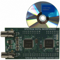
Manufacturer Part Number
DC-VIDEO-TVP5146N
Description
VIDEO DAUGHTER CARD
Manufacturer
Altera
Series
Stratix® IIIr
Datasheets
1.EP3SL150F780C4N.pdf
(16 pages)
2.EP3SL150F780C4N.pdf
(332 pages)
3.DC-VIDEO-TVP5146N.pdf
(58 pages)
Specifications of DC-VIDEO-TVP5146N
Main Purpose
Video, Daughter Card
Embedded
No
Utilized Ic / Part
Altera Dev Kits
Primary Attributes
Dual Composite Video Input - NTSC or PAL
Secondary Attributes
10-bit BT.656 Output, Compatible with Expansion Connector, Standard on Most Altera Development Kits
Lead Free Status / RoHS Status
Lead free / RoHS Compliant
Other names
544-1704


1–328
Table 1.
Stratix III Device Handbook, Volume 2
Glossary Table (Part 3 of 4)
Letter
S
T
U
to-channel-skew)
TCCS (channel-
Referenced I/O
SW (sampling
Single-ended
t
t
Standard
O U T P J _ D C
window)
O U T P J _ I O
Voltage
Subject
t
t
t
t
IN C C J
D U T Y
F A L L
R I S E
—
t
C
The period of time during which the data must be valid in order to capture it correctly. The
setup and hold times determine the ideal strobe position within the sampling window (the
following figure):
Timing Diagram
The JEDEC standard for SSTl and HSTL I/O standards defines both the AC and DC input
signal values. The AC values indicate the voltage levels at which the receiver must meet its
timing specifications. The DC values indicate the voltage levels at which the final logic state of
the receiver is unambiguously defined. After the receiver input has crossed the AC value, the
receiver changes to the new logic state.
The new logic state is maintained as long as the input stays beyond the DC threshold. This
approach is intended to provide predictable receiver timing in the presence of input waveform
ringing (The following figure):
Single-Ended Voltage Referenced I/O Standard
High-Speed receiver/transmitter input and output clock period.
The timing difference between the fastest and slowest output edges, including t
and clock skew, across channels driven by the same PLL. The clock is included in the TCCS
measurement (refer to the Timing Diagram figure under S in this table)
High-Speed I/O Block: Duty cycle on high-speed transmitter output clock.
Timing Unit Interval (TUI)
The timing budget allowed for skew, propagation delays, and data sampling window. (TUI =
1/(Receiver Input Clock Frequency Multiplication Factor) = t
Signal high-to-low transition time (80-20%)
Cycle-to-cycle jitter tolerance on PLL clock input
Period jitter on general purpose I/O driven by a PLL
Period jitter on dedicated clock output driven by a PLL
Signal low-to-high transition time (20-80%)
V
V
OH
OL
0.5 x TCCS
Chapter 1: Stratix III Device Datasheet: DC and Switching Characteristics
RSKM
Definitions
Sampling Window
V
Bit Time
REF
(SW)
—
RSKM
C
/w)
V
V
© July 2010 Altera Corporation
IH(DC)
IL(DC)
0.5 x TCCS
V
V
IH ( AC )
IL(AC )
V
CCIO
V
co
SS
variation
Glossary
Related parts for DC-VIDEO-TVP5146N
Image
Part Number
Description
Manufacturer
Datasheet
Request
R

Part Number:
Description:
CYCLONE II STARTER KIT EP2C20N
Manufacturer:
Altera
Datasheet:


Part Number:
Description:
CPLD, EP610 Family, ECMOS Process, 300 Gates, 16 Macro Cells, 16 Reg., 16 User I/Os, 5V Supply, 35 Speed Grade, 24DIP
Manufacturer:
Altera Corporation
Datasheet:
Part Number:
Description:
CPLD, EP610 Family, ECMOS Process, 300 Gates, 16 Macro Cells, 16 Reg., 16 User I/Os, 5V Supply, 15 Speed Grade, 24DIP
Manufacturer:
Altera Corporation
Datasheet:
Part Number:
Description:
Manufacturer:
Altera Corporation
Datasheet:
Part Number:
Description:
CPLD, EP610 Family, ECMOS Process, 300 Gates, 16 Macro Cells, 16 Reg., 16 User I/Os, 5V Supply, 30 Speed Grade, 24DIP
Manufacturer:
Altera Corporation
Datasheet:
Part Number:
Description:
High-performance, low-power erasable programmable logic devices with 8 macrocells, 10ns
Manufacturer:
Altera Corporation
Datasheet:
Part Number:
Description:
High-performance, low-power erasable programmable logic devices with 8 macrocells, 7ns
Manufacturer:
Altera Corporation
Datasheet:
Part Number:
Description:
Classic EPLD
Manufacturer:
Altera Corporation
Datasheet:
Part Number:
Description:
High-performance, low-power erasable programmable logic devices with 8 macrocells, 10ns
Manufacturer:
Altera Corporation
Datasheet:
Part Number:
Description:
Manufacturer:
Altera Corporation
Datasheet:
Part Number:
Description:
Manufacturer:
Altera Corporation
Datasheet:
Part Number:
Description:
Manufacturer:
Altera Corporation
Datasheet:
Part Number:
Description:
CPLD, EP610 Family, ECMOS Process, 300 Gates, 16 Macro Cells, 16 Reg., 16 User I/Os, 5V Supply, 25 Speed Grade, 24DIP
Manufacturer:
Altera Corporation
Datasheet: