DC-VIDEO-TVP5146N Altera, DC-VIDEO-TVP5146N Datasheet - Page 31
DC-VIDEO-TVP5146N
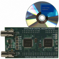
Manufacturer Part Number
DC-VIDEO-TVP5146N
Description
VIDEO DAUGHTER CARD
Manufacturer
Altera
Series
Stratix® IIIr
Datasheets
1.EP3SL150F780C4N.pdf
(16 pages)
2.EP3SL150F780C4N.pdf
(332 pages)
3.DC-VIDEO-TVP5146N.pdf
(58 pages)
Specifications of DC-VIDEO-TVP5146N
Main Purpose
Video, Daughter Card
Embedded
No
Utilized Ic / Part
Altera Dev Kits
Primary Attributes
Dual Composite Video Input - NTSC or PAL
Secondary Attributes
10-bit BT.656 Output, Compatible with Expansion Connector, Standard on Most Altera Development Kits
Lead Free Status / RoHS Status
Lead free / RoHS Compliant
Other names
544-1704


Chapter 1: Stratix III Device Datasheet: DC and Switching Characteristics
I/O Timing
Preliminary and Final Timing
I/O Timing Measurement Methodology
© July 2010 Altera Corporation
Timing models can have either preliminary or final status. The Quartus II software
issues an informational message during design compilation if the timing models are
preliminary.
Preliminary status means that the timing models are subject to change in future
Quartus II releases. Initially, timing numbers are created using simulation results,
process data, and other known parameters. Parts of the timing models may be
correlated to silicon measurements. Various tests are used to make the preliminary
numbers as close to the actual timing parameters as possible.
Final timing models are based on simulation models that are characterized versus the
actual device measurements under all allowable operating conditions. When the
timing models are final, all or most of the Stratix III family devices have been
completely characterized and no further changes to the timing model are expected.
Table 1–36. Timing Model Status for Stratix III Devices
Altera characterizes timing delays at the worst-case process, minimum voltage, and
maximum temperature for input register setup time (t
Quartus II software uses the following equations to calculate t
Stratix III devices input signals.
t
+ data delay from the input pin to the input register
+ micro setup time of the input register
- clock delay from the input pin to the input register
t
- data delay from the input pin to the input register
+ micro hold time of the input register
+ clock delay from the input pin to the input register
su
h
EP3SL50
EP3SL70
EP3SL110
EP3SL150
EP3SL200
EP3SL340
EP3SE50
EP3SE80
EP3SE110
EP3SE260
=
=
Table 1–36
Device
lists the status of the Stratix III device timing models.
Preliminary
—
—
—
—
—
—
—
—
—
—
su
) and hold time (t
Stratix III Device Handbook, Volume 2
su
and t
h
timing for the
h
Final
). The
v
v
v
v
v
v
v
v
v
v
1–31
Related parts for DC-VIDEO-TVP5146N
Image
Part Number
Description
Manufacturer
Datasheet
Request
R

Part Number:
Description:
CYCLONE II STARTER KIT EP2C20N
Manufacturer:
Altera
Datasheet:


Part Number:
Description:
CPLD, EP610 Family, ECMOS Process, 300 Gates, 16 Macro Cells, 16 Reg., 16 User I/Os, 5V Supply, 35 Speed Grade, 24DIP
Manufacturer:
Altera Corporation
Datasheet:
Part Number:
Description:
CPLD, EP610 Family, ECMOS Process, 300 Gates, 16 Macro Cells, 16 Reg., 16 User I/Os, 5V Supply, 15 Speed Grade, 24DIP
Manufacturer:
Altera Corporation
Datasheet:
Part Number:
Description:
Manufacturer:
Altera Corporation
Datasheet:
Part Number:
Description:
CPLD, EP610 Family, ECMOS Process, 300 Gates, 16 Macro Cells, 16 Reg., 16 User I/Os, 5V Supply, 30 Speed Grade, 24DIP
Manufacturer:
Altera Corporation
Datasheet:
Part Number:
Description:
High-performance, low-power erasable programmable logic devices with 8 macrocells, 10ns
Manufacturer:
Altera Corporation
Datasheet:
Part Number:
Description:
High-performance, low-power erasable programmable logic devices with 8 macrocells, 7ns
Manufacturer:
Altera Corporation
Datasheet:
Part Number:
Description:
Classic EPLD
Manufacturer:
Altera Corporation
Datasheet:
Part Number:
Description:
High-performance, low-power erasable programmable logic devices with 8 macrocells, 10ns
Manufacturer:
Altera Corporation
Datasheet:
Part Number:
Description:
Manufacturer:
Altera Corporation
Datasheet:
Part Number:
Description:
Manufacturer:
Altera Corporation
Datasheet:
Part Number:
Description:
Manufacturer:
Altera Corporation
Datasheet:
Part Number:
Description:
CPLD, EP610 Family, ECMOS Process, 300 Gates, 16 Macro Cells, 16 Reg., 16 User I/Os, 5V Supply, 25 Speed Grade, 24DIP
Manufacturer:
Altera Corporation
Datasheet: