NCP1605FORWGEVB ON Semiconductor, NCP1605FORWGEVB Datasheet - Page 10
NCP1605FORWGEVB
Manufacturer Part Number
NCP1605FORWGEVB
Description
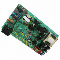
EVAL BOARD FOR NCP1605FORWG
Manufacturer
ON Semiconductor
Datasheets
1.NCP1217P100G.pdf
(19 pages)
2.NCP1605ADR2G.pdf
(32 pages)
3.NCP1605FORWGEVB.pdf
(2 pages)
4.NCP1605FORWGEVB.pdf
(20 pages)
Specifications of NCP1605FORWGEVB
Design Resources
NCP1605FORWGEVB BOM NCP1605FORWGEVB Gerber Files NCP1605 EVB Schematic
Main Purpose
AC/DC, Primary and Secondary Side with PFC
Outputs And Type
1, Isolated
Voltage - Output
19V
Current - Output
8A
Voltage - Input
90 ~ 265VAC
Regulator Topology
Forward Converter
Frequency - Switching
133kHz
Board Type
Fully Populated
Utilized Ic / Part
NCP1217, NCP1605
Lead Free Status / RoHS Status
Lead free / RoHS Compliant
Power - Output
-
Lead Free Status / Rohs Status
Lead free / RoHS Compliant
For Use With/related Products
NCP1605FORWG
Other names
NCP1605FORWGEVBOS


Calculating the V
consumption as soon as V
NCP1217P065 is used and drives a MOSFET with a 30 nC
total gate charge (Qg). The total average current is thus
made of ICC1 (750 mA) plus the driver current,
The ΔV available to fully startup the circuit (e.g. never reach
the 8.2 V VCC
best case or 4.9 V worse case
capacitor that then needs to supply the NCP1217 with
2.7 mA during a given time until the auxiliary supply takes
over. Suppose that this time was measured at around 15 ms.
CV
Skipping Cycle Mode
the output power demand drops below a given level. This is
accomplished by monitoring the FB pin. In normal
operation, pin 2 imposes a peak current accordingly to the
load value. If the load demand decreases, the internal loop
asks for less peak current. When this setpoint reaches a
determined level (Vpin 1), the IC prevents the current from
decreasing further down and starts to blank the output
pulses: the IC enters the so- -called skip cycle mode, also
named controlled burst operation. The power transfer now
depends upon the width of the pulse bunches (Figure 20).
Suppose we have the following component values:
Lp, primary inductance = 350 mH
Fsw, switching frequency = 65 kHz
Ip skip = 600 mA (or 333 mV/Rsense)
Fsw * Qg = 1.95 mA
C ≥ 8.3 mF.
The V
The NCP1217 automatically skips switching cycles when
CC
is calculated using the equation
CC
capacitor can be calculated knowing the IC
Select a 22 mF/25 V and this will fit.
min
CC
during power on) is
. The total current is therefore 2.7 mA.
Capacitor
CC
VCC
reaches 12.8 V. Suppose that a
Figure 18. Typical Waveforms in Short Circuit Conditions
ON
(11.9--7.0)
= 12.8 V
13.7--8.2 = 5.5 V
VCC
. We have a
VCC
C =
latch
min
Δt · i
= 5.6 V
ΔV
http://onsemi.com
= 7.6 V
or
10
mode with a bunch length of 10 ms over a recurrent
period of 100 ms, then the total power transfer is:
a look at the operation mode versus the FB level
immediately gives the necessary insight.
default), the peak current cannot exceed 1.0 V/Rsense.
When the IC enters the skip cycle mode, the peak current
cannot go below Vpin1/3.3. The user still has the flexibility
to alter this 1.0 V by either shunting pin 1 to ground through
a resistor or raising it through a resistor up to the desired
level. In this later case, care must be taken to keep sufficient
margin between this pin 1 adjustment level and the latchoff
level. Grounding pin 1 permanently invalidates the skip
cycle operation.
1
2
4.1 * 0.1 = 410 mW
FB
DRIVING PULSES
The
To better understand how this skip cycle mode takes place,
When FB is above the skip cycle threshold (1.0 V by
· Lp · Ip 2 · Fsw = 4.1 W
NORMAL CURRENT
MODE OPERATION
SKIP CYCLE OPERATION
I
P(min)
V
CC
theoretical
= 333 mV/R
.
SENSE
power
Figure 19.
. If this IC enters skip cycle
transfer
4.2 V, FB Pin Open
3.2 V, Upper
Dynamic Range
1 V
is
therefore:
Time
Related parts for NCP1605FORWGEVB
Image
Part Number
Description
Manufacturer
Datasheet
Request
R

Part Number:
Description:
ON Semiconductor [VOLTAGE REGULATOR]
Manufacturer:
ON Semiconductor
Datasheet:
Part Number:
Description:
357-036-542-201 CARDEDGE 36POS DL .156 BLK LOPRO
Manufacturer:
ON Semiconductor
Datasheet:
Part Number:
Description:
357-036-542-201 CARDEDGE 36POS DL .156 BLK LOPRO
Manufacturer:
ON Semiconductor
Datasheet:
Part Number:
Description:
357-036-542-201 CARDEDGE 36POS DL .156 BLK LOPRO
Manufacturer:
ON Semiconductor
Datasheet:
Part Number:
Description:
357-036-542-201 CARDEDGE 36POS DL .156 BLK LOPRO
Manufacturer:
ON Semiconductor
Datasheet:
Part Number:
Description:
357-036-542-201 CARDEDGE 36POS DL .156 BLK LOPRO
Manufacturer:
ON Semiconductor
Datasheet:
Part Number:
Description:
357-036-542-201 CARDEDGE 36POS DL .156 BLK LOPRO
Manufacturer:
ON Semiconductor
Datasheet:
Part Number:
Description:
357-036-542-201 CARDEDGE 36POS DL .156 BLK LOPRO
Manufacturer:
ON Semiconductor
Datasheet:
Part Number:
Description:
357-036-542-201 CARDEDGE 36POS DL .156 BLK LOPRO
Manufacturer:
ON Semiconductor
Datasheet:
Part Number:
Description:
357-036-542-201 CARDEDGE 36POS DL .156 BLK LOPRO
Manufacturer:
ON Semiconductor
Datasheet:
Part Number:
Description:
357-036-542-201 CARDEDGE 36POS DL .156 BLK LOPRO
Manufacturer:
ON Semiconductor
Datasheet:
Part Number:
Description:
Manufacturer:
ON Semiconductor
Datasheet:
Part Number:
Description:
Manufacturer:
ON Semiconductor
Datasheet:
Part Number:
Description:
Manufacturer:
ON Semiconductor
Datasheet: