NCP1605FORWGEVB ON Semiconductor, NCP1605FORWGEVB Datasheet - Page 9
NCP1605FORWGEVB
Manufacturer Part Number
NCP1605FORWGEVB
Description
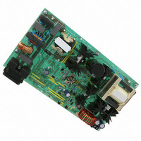
EVAL BOARD FOR NCP1605FORWG
Manufacturer
ON Semiconductor
Datasheets
1.NCP1217P100G.pdf
(19 pages)
2.NCP1605ADR2G.pdf
(32 pages)
3.NCP1605FORWGEVB.pdf
(2 pages)
4.NCP1605FORWGEVB.pdf
(20 pages)
Specifications of NCP1605FORWGEVB
Design Resources
NCP1605FORWGEVB BOM NCP1605FORWGEVB Gerber Files NCP1605 EVB Schematic
Main Purpose
AC/DC, Primary and Secondary Side with PFC
Outputs And Type
1, Isolated
Voltage - Output
19V
Current - Output
8A
Voltage - Input
90 ~ 265VAC
Regulator Topology
Forward Converter
Frequency - Switching
133kHz
Board Type
Fully Populated
Utilized Ic / Part
NCP1217, NCP1605
Lead Free Status / RoHS Status
Lead free / RoHS Compliant
Power - Output
-
Lead Free Status / Rohs Status
Lead free / RoHS Compliant
For Use With/related Products
NCP1605FORWG
Other names
NCP1605FORWGEVBOS


Startup Sequence
outlet, the internal current source (typically 7.0 mA) is
biased and charges up the V
on this V
constrained below 16 V, which is the maximum rating on
Pin 6. Figure 17 portrays a typical startup sequence with a
V
Overload Operation
controlled (e.g. wall adapters delivering raw DC level), it is
interesting to implement a true short- -circuit protection. A
short- -circuit actually forces the output voltage to be at a low
CC
13.5
12.5
10.5
When the power supply is first powered from the mains
Once the power supply has started, the V
11.5
In applications where the output current is purposely not
9.5
regulated at 12.5 V.
Figure 17. A Typical Startup Sequence for
3.00 M
CC
capacitor reaches the VCC
12.8 V
8.00 M
12.8 V/5.6 V
Figure 16. The Current Source Brings V
the NCP1217
t, TIME (sec)
CC
13.0 M
capacitor. When the voltage
+
--
18.0 M
ON
level (typically
REGULATION
CC
23.0 M
shall be
http://onsemi.com
6 mA or 0
9
CC
12.8 V), the current source turns off and no longer wastes
any power. At this time, the V
controller and the auxiliary supply is supposed to take over
before V
internal arrangement of this structure.
level, preventing a bias current to circulate in the
optocoupler LED. As a result, the auxiliary voltage also
decreases because it also operates in Flyback and thus
duplicates the output voltage, providing the leakage
inductance between windings is kept low. To account for this
situation and properly protect the power supply, NCP1217
hosts a dedicated overload detection circuitry. Once
activated, this circuitry imposes to deliver pulses in a burst
manner with a low duty- -cycle. The system auto- -recovers
when the fault condition disappears.
maximum until the output voltage reaches its target and the
feedback loop takes over. The auxiliary voltage takes place
after a few switching cycles and self- -supplies the IC. In
presence of a short circuit on the output, the auxiliary
voltage will go down until it crosses the undervoltage
lockout level of typically 7.6 V. When this happens,
NCP1217 immediately stops the switching pulses and
unbiases all unnecessary logical blocks. The overall
consumption drops, while keeping the gate grounded, and
the V
5.6 V, the startup source turns- -on again and a new startup
sequence occurs, bringing V
to restart. If the default has gone, then the power supply
normally restarts. If not, a new protective burst is initiated,
shielding the SMPS from any runaway. Figure 18 portrays
the typical operating signals in short circuit.
8
6
4
Above 12.8 V and then Turns Off
During the startup phase, the peak current is pushed to the
CC
slowly falls down. As soon as V
CC
CV
collapses below VCC
CC
HV
Aux
CC
CC
toward 12.8 V as an attempt
capacitor only supplies the
min
. Figure 16 shows the
CC
reaches typically
Related parts for NCP1605FORWGEVB
Image
Part Number
Description
Manufacturer
Datasheet
Request
R

Part Number:
Description:
ON Semiconductor [VOLTAGE REGULATOR]
Manufacturer:
ON Semiconductor
Datasheet:
Part Number:
Description:
357-036-542-201 CARDEDGE 36POS DL .156 BLK LOPRO
Manufacturer:
ON Semiconductor
Datasheet:
Part Number:
Description:
357-036-542-201 CARDEDGE 36POS DL .156 BLK LOPRO
Manufacturer:
ON Semiconductor
Datasheet:
Part Number:
Description:
357-036-542-201 CARDEDGE 36POS DL .156 BLK LOPRO
Manufacturer:
ON Semiconductor
Datasheet:
Part Number:
Description:
357-036-542-201 CARDEDGE 36POS DL .156 BLK LOPRO
Manufacturer:
ON Semiconductor
Datasheet:
Part Number:
Description:
357-036-542-201 CARDEDGE 36POS DL .156 BLK LOPRO
Manufacturer:
ON Semiconductor
Datasheet:
Part Number:
Description:
357-036-542-201 CARDEDGE 36POS DL .156 BLK LOPRO
Manufacturer:
ON Semiconductor
Datasheet:
Part Number:
Description:
357-036-542-201 CARDEDGE 36POS DL .156 BLK LOPRO
Manufacturer:
ON Semiconductor
Datasheet:
Part Number:
Description:
357-036-542-201 CARDEDGE 36POS DL .156 BLK LOPRO
Manufacturer:
ON Semiconductor
Datasheet:
Part Number:
Description:
357-036-542-201 CARDEDGE 36POS DL .156 BLK LOPRO
Manufacturer:
ON Semiconductor
Datasheet:
Part Number:
Description:
357-036-542-201 CARDEDGE 36POS DL .156 BLK LOPRO
Manufacturer:
ON Semiconductor
Datasheet:
Part Number:
Description:
Manufacturer:
ON Semiconductor
Datasheet:
Part Number:
Description:
Manufacturer:
ON Semiconductor
Datasheet:
Part Number:
Description:
Manufacturer:
ON Semiconductor
Datasheet: