NCP1605FORWGEVB ON Semiconductor, NCP1605FORWGEVB Datasheet - Page 15
NCP1605FORWGEVB
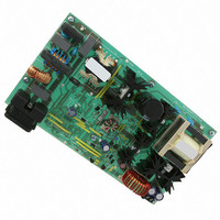
Manufacturer Part Number
NCP1605FORWGEVB
Description
EVAL BOARD FOR NCP1605FORWG
Manufacturer
ON Semiconductor
Datasheets
1.NCP1217P100G.pdf
(19 pages)
2.NCP1605ADR2G.pdf
(32 pages)
3.NCP1605FORWGEVB.pdf
(2 pages)
4.NCP1605FORWGEVB.pdf
(20 pages)
Specifications of NCP1605FORWGEVB
Design Resources
NCP1605FORWGEVB BOM NCP1605FORWGEVB Gerber Files NCP1605 EVB Schematic
Main Purpose
AC/DC, Primary and Secondary Side with PFC
Outputs And Type
1, Isolated
Voltage - Output
19V
Current - Output
8A
Voltage - Input
90 ~ 265VAC
Regulator Topology
Forward Converter
Frequency - Switching
133kHz
Board Type
Fully Populated
Utilized Ic / Part
NCP1217, NCP1605
Lead Free Status / RoHS Status
Lead free / RoHS Compliant
Power - Output
-
Lead Free Status / Rohs Status
Lead free / RoHS Compliant
For Use With/related Products
NCP1605FORWG
Other names
NCP1605FORWGEVBOS


internal parasitic SCR activation. One of them consists in
inserting a resistor in series with the high- -voltage pin to
keep the negative current to the lowest when the bulk
becomes negative (Figure 28). Please note that the negative
spike is clamped to (- -2*Vf) thanks to the diode bridge. Also,
the power dissipation of this resistor is extremely small since
it only heats up during the startup sequence.
Simple and inexpensive cures exist to prevent from
Figure 28. A simple resistor in series avoids any
Figure 27. A Negative Spike Takes Place on the Bulk Capacitor at the Switch- -Off Sequence
+
Cbulk
latch- -up in the controller . . .
1
2
3
4
Vcc 5 V/DIV
Vlatch 1 V/DIV
Time 10 ms/DIV
8
7
6
5
2
3
1
+
Rbulk
>4.7 k
CV
http://onsemi.com
CC
15
from V
VCC
the bulk capacitor gets deeply discharged. For security
reasons, two diodes can be connected in series.
Another option (Figure 29) consists in wiring a diode
Figure 29. . . . or one diode forces V
ON
CC
sooner and thus stops the switching activity before
to the bulk capacitor to force V
+
Cbulk
VCC
1
2
3
4
ON
sooner.
8
7
6
5
3
CC
to reach
CC
1
+
D3
1N4007
CV
to reach
CC
Related parts for NCP1605FORWGEVB
Image
Part Number
Description
Manufacturer
Datasheet
Request
R

Part Number:
Description:
ON Semiconductor [VOLTAGE REGULATOR]
Manufacturer:
ON Semiconductor
Datasheet:
Part Number:
Description:
357-036-542-201 CARDEDGE 36POS DL .156 BLK LOPRO
Manufacturer:
ON Semiconductor
Datasheet:
Part Number:
Description:
357-036-542-201 CARDEDGE 36POS DL .156 BLK LOPRO
Manufacturer:
ON Semiconductor
Datasheet:
Part Number:
Description:
357-036-542-201 CARDEDGE 36POS DL .156 BLK LOPRO
Manufacturer:
ON Semiconductor
Datasheet:
Part Number:
Description:
357-036-542-201 CARDEDGE 36POS DL .156 BLK LOPRO
Manufacturer:
ON Semiconductor
Datasheet:
Part Number:
Description:
357-036-542-201 CARDEDGE 36POS DL .156 BLK LOPRO
Manufacturer:
ON Semiconductor
Datasheet:
Part Number:
Description:
357-036-542-201 CARDEDGE 36POS DL .156 BLK LOPRO
Manufacturer:
ON Semiconductor
Datasheet:
Part Number:
Description:
357-036-542-201 CARDEDGE 36POS DL .156 BLK LOPRO
Manufacturer:
ON Semiconductor
Datasheet:
Part Number:
Description:
357-036-542-201 CARDEDGE 36POS DL .156 BLK LOPRO
Manufacturer:
ON Semiconductor
Datasheet:
Part Number:
Description:
357-036-542-201 CARDEDGE 36POS DL .156 BLK LOPRO
Manufacturer:
ON Semiconductor
Datasheet:
Part Number:
Description:
357-036-542-201 CARDEDGE 36POS DL .156 BLK LOPRO
Manufacturer:
ON Semiconductor
Datasheet:
Part Number:
Description:
Manufacturer:
ON Semiconductor
Datasheet:
Part Number:
Description:
Manufacturer:
ON Semiconductor
Datasheet:
Part Number:
Description:
Manufacturer:
ON Semiconductor
Datasheet: