NCP1605FORWGEVB ON Semiconductor, NCP1605FORWGEVB Datasheet - Page 3
NCP1605FORWGEVB
Manufacturer Part Number
NCP1605FORWGEVB
Description
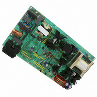
EVAL BOARD FOR NCP1605FORWG
Manufacturer
ON Semiconductor
Datasheets
1.NCP1217P100G.pdf
(19 pages)
2.NCP1605ADR2G.pdf
(32 pages)
3.NCP1605FORWGEVB.pdf
(2 pages)
4.NCP1605FORWGEVB.pdf
(20 pages)
Specifications of NCP1605FORWGEVB
Design Resources
NCP1605FORWGEVB BOM NCP1605FORWGEVB Gerber Files NCP1605 EVB Schematic
Main Purpose
AC/DC, Primary and Secondary Side with PFC
Outputs And Type
1, Isolated
Voltage - Output
19V
Current - Output
8A
Voltage - Input
90 ~ 265VAC
Regulator Topology
Forward Converter
Frequency - Switching
133kHz
Board Type
Fully Populated
Utilized Ic / Part
NCP1217, NCP1605
Lead Free Status / RoHS Status
Lead free / RoHS Compliant
Power - Output
-
Lead Free Status / Rohs Status
Lead free / RoHS Compliant
For Use With/related Products
NCP1605FORWG
Other names
NCP1605FORWGEVBOS


Stresses exceeding Maximum Ratings may damage the device. Maximum Ratings are stress ratings only. Functional operation above the
Recommended Operating Conditions is not implied. Extended exposure to stresses above the Recommended Operating Conditions may affect
device reliability.
MAXIMUM RATINGS
Power Supply Voltage
Power Supply Voltage on All Other Pins Except Pin 8 (HV), Pin 6 (V
Maximum Voltage on Pin 8 (HV), Pin 6 (V
Maximum Voltage on Pin 8 (HV), Pin 6 (V
Minimum Operating Voltage on Pin 8 (HV)
Maximum Current into All Pins Except V
Thermal Resistance, Junction--to--Case
Thermal Resistance, Junction--to--Air, PDIP--7 Version
Thermal Resistance, Junction--to--Air, SO--8 Version
Maximum Junction Temperature
Temperature Shutdown
Hysteresis in Shutdown
Storage Temperature Range
ESD Capability, HBM Model (All Pins Except V
ESD Capability, Machine Model
Current
Ground
Sense
Adj
FB
1
2
3
4
* Available for “A” version only
20 k
Compensation
+
--
V
250 ns
L.E.B.
Ramp
REF
80 k
19 k
57 k
25 k
1.1 V
24 k
CC
CC
CC
(6) and HV (8) when 10 V ESD Diodes are Activated
65--100--133 kHz
) Decoupled to Ground with 10 mF
) Grounded
Rating
Figure 2. Internal Circuit Architecture
CC
+
--
Clock
and HV)
1 V
+
--
+
--
3.1 V
+
--
Latchoff
Comparator
Skip Cycle
Comparator
http://onsemi.com
1ms SS*
Set
3
CC
Reset
) and Pin 5 (Drv)
DCmax = 74%
Latch
Q Flip--Flop
Internal V
Reset
Set
Reset
CC
Q
UVLO
UVLO High and Low
Symbol
500 mA
T
R
R
R
V
V
V
JMAX
Management
θJC
θJA
θJA
CC
--
HV
HV
--
--
--
--
--
--
Overload
HV Current
--60 to +150
--0.3 to 10
Value
Source
500
450
100
178
150
155
200
5.0
2.0
16
28
57
30
C/W
C/W
Unit
mA
C
C
C
C
kV
HV
NC
V
Drv
8
7
6
5
V
V
V
V
V
V
CC
Related parts for NCP1605FORWGEVB
Image
Part Number
Description
Manufacturer
Datasheet
Request
R

Part Number:
Description:
ON Semiconductor [VOLTAGE REGULATOR]
Manufacturer:
ON Semiconductor
Datasheet:
Part Number:
Description:
357-036-542-201 CARDEDGE 36POS DL .156 BLK LOPRO
Manufacturer:
ON Semiconductor
Datasheet:
Part Number:
Description:
357-036-542-201 CARDEDGE 36POS DL .156 BLK LOPRO
Manufacturer:
ON Semiconductor
Datasheet:
Part Number:
Description:
357-036-542-201 CARDEDGE 36POS DL .156 BLK LOPRO
Manufacturer:
ON Semiconductor
Datasheet:
Part Number:
Description:
357-036-542-201 CARDEDGE 36POS DL .156 BLK LOPRO
Manufacturer:
ON Semiconductor
Datasheet:
Part Number:
Description:
357-036-542-201 CARDEDGE 36POS DL .156 BLK LOPRO
Manufacturer:
ON Semiconductor
Datasheet:
Part Number:
Description:
357-036-542-201 CARDEDGE 36POS DL .156 BLK LOPRO
Manufacturer:
ON Semiconductor
Datasheet:
Part Number:
Description:
357-036-542-201 CARDEDGE 36POS DL .156 BLK LOPRO
Manufacturer:
ON Semiconductor
Datasheet:
Part Number:
Description:
357-036-542-201 CARDEDGE 36POS DL .156 BLK LOPRO
Manufacturer:
ON Semiconductor
Datasheet:
Part Number:
Description:
357-036-542-201 CARDEDGE 36POS DL .156 BLK LOPRO
Manufacturer:
ON Semiconductor
Datasheet:
Part Number:
Description:
357-036-542-201 CARDEDGE 36POS DL .156 BLK LOPRO
Manufacturer:
ON Semiconductor
Datasheet:
Part Number:
Description:
Manufacturer:
ON Semiconductor
Datasheet:
Part Number:
Description:
Manufacturer:
ON Semiconductor
Datasheet:
Part Number:
Description:
Manufacturer:
ON Semiconductor
Datasheet: