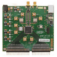
DAC1405D750/DB,598 NXP Semiconductors, DAC1405D750/DB,598 Datasheet - Page 14

DAC1405D750/DB,598
Manufacturer Part Number
DAC1405D750/DB,598
Description
BOARD DEMO FOR DAC1405D750
Manufacturer
NXP Semiconductors
Type
D/Ar
Datasheets
1.DAC1405D750HWC15.pdf
(42 pages)
2.HSDC-ACC01DB.pdf
(32 pages)
3.ADC1415S125DB598.pdf
(2 pages)
Specifications of DAC1405D750/DB,598
Number Of Dac's
2
Number Of Bits
14
Outputs And Type
2, Differential
Sampling Rate (per Second)
750M
Data Interface
Serial, SPI™
Settling Time
20ns
Dac Type
Current
Voltage Supply Source
Analog and Digital
Operating Temperature
-40°C ~ 85°C
Utilized Ic / Part
DAC1405D750
Product
Data Conversion Development Tools
Conversion Rate
750 MSPS
Resolution
14 bit
Interface Type
SMA
Supply Voltage (max)
3.3 V
Supply Voltage (min)
1.8 V
For Use With/related Products
DAC1405D750
Lead Free Status / RoHS Status
Lead free / RoHS Compliant
Lead Free Status / RoHS Status
Lead free / RoHS Compliant, Lead free / RoHS Compliant
Other names
568-5090
NXP Semiconductors
DAC1405D750
Product data sheet
Fig 3.
RESET_N
(optional)
SCS_N
SCLK
SDIO
SDO
R/W indicates the mode access, (see
SPI protocol
10.2.2 SPI timing description
R/W
Table 6.
In
Table 7.
A0 to A4: indicate which register is being addressed. In the case of a multiple transfer, this
address concerns the first register after which the next registers follow directly in a
decreasing order according to
The interface can operate at a frequency of up to 15 MHz. The SPI timing is shown in
Figure
R/W
N1
0
0
1
1
0
1
N1
Fig 4.
Table 7
RESET_N
N0
4.
SCS_N
SCLK
SDIO
SPI timing diagram
N1 and N0 indicate the number of bytes transferred after the instruction byte.
Read or Write mode access description
Number of bytes transferred
A4
All information provided in this document is subject to legal disclaimers.
A3
Table
Description
Write mode operation
Read mode operation
50 %
50 %
N0
0
1
0
1
50 %
Rev. 3 — 7 September 2010
6)
A2
t
w(RESET_N)
50 %
A1
Dual 14-bit DAC, up to 750 Msps; 4 and 8 interpolating
Table 9 “Register allocation
t
t
su(SCS_N)
su(SDIO)
A0
t
h(SDIO)
D7
D7
Number of bytes
1 byte transferred
2 bytes transferred
3 bytes transferred
4 bytes transferred
D6
D6
D5
D5
t
w(SCLK)
D4
D4
map”.
DAC1405D750
D3
D3
D2
D2
© NXP B.V. 2010. All rights reserved.
D1
D1
D0
D0
t
001aaj813
h(SCS_N)
001aaj812
14 of 42


