DAC1405D750/DB,598 NXP Semiconductors, DAC1405D750/DB,598 Datasheet - Page 22
DAC1405D750/DB,598
Manufacturer Part Number
DAC1405D750/DB,598
Description
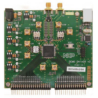
BOARD DEMO FOR DAC1405D750
Manufacturer
NXP Semiconductors
Type
D/Ar
Datasheets
1.DAC1405D750HWC15.pdf
(42 pages)
2.HSDC-ACC01DB.pdf
(32 pages)
3.ADC1415S125DB598.pdf
(2 pages)
Specifications of DAC1405D750/DB,598
Number Of Dac's
2
Number Of Bits
14
Outputs And Type
2, Differential
Sampling Rate (per Second)
750M
Data Interface
Serial, SPI™
Settling Time
20ns
Dac Type
Current
Voltage Supply Source
Analog and Digital
Operating Temperature
-40°C ~ 85°C
Utilized Ic / Part
DAC1405D750
Product
Data Conversion Development Tools
Conversion Rate
750 MSPS
Resolution
14 bit
Interface Type
SMA
Supply Voltage (max)
3.3 V
Supply Voltage (min)
1.8 V
For Use With/related Products
DAC1405D750
Lead Free Status / RoHS Status
Lead free / RoHS Compliant
Lead Free Status / RoHS Status
Lead free / RoHS Compliant, Lead free / RoHS Compliant
Other names
568-5090


NXP Semiconductors
DAC1405D750
Product data sheet
10.2.5 Recommended configuration
10.3.1 Dual-port mode
10.3.2 Interleaved mode
10.3 Input data
It is recommended that the following additional settings are used to obtain optimum
performance at up to 750 Msps.
Table 31.
The setting applied to MODE_SEL (register 00h[3]; see
whether the DAC1405D750 operates in the Dual-port mode or in Interleaved mode (see
Table
Table 32.
The data input for Dual-port mode operation is shown in
DAC has its own independent data input. The data enters the input latch on the rising
edge of the internal clock signal and is transferred to the DAC latch.
The data input for the Interleaved mode operation is illustrated in
mode
Address
Dec
17
19
20
Bit 3 setting
0
1
Fig 5.
32).
operation”.
Dual-port mode
Recommended configuration
Mode selection
Q13 to Q0
Function
Dual port mode
Interleaved mode
All information provided in this document is subject to legal disclaimers.
I13 to I0
Hex
11h
13h
14h
Rev. 3 — 7 September 2010
Dual 14-bit DAC, up to 750 Msps; 4 and 8 interpolating
LATCH
LATCH
Q
I
01101100
Value
Bin
00001010
01101100
active
I13 to I0
active
2 ×
2 ×
FIR 1
FIR 1
2 ×
2 ×
FIR 2
FIR 2
Dec
10
108
108
Q13 to Q0
active
off
Table 10 on page
Figure 5 “Dual-port
DAC1405D750
2 ×
2 ×
Figure 6 “Interleaved
FIR 3
FIR 3
001aal653
© NXP B.V. 2010. All rights reserved.
Pin 41
Q13
SELIQ
Hex
0Ah
6Ch
6Ch
17) defines
mode”. Each
22 of 42
Related parts for DAC1405D750/DB,598
Image
Part Number
Description
Manufacturer
Datasheet
Request
R

Part Number:
Description:
Dual 14-bit Dac, Up To 750 Msps; 4 And 8 Interpolating
Manufacturer:
NXP Semiconductors
Datasheet:
Part Number:
Description:
NXP Semiconductors designed the LPC2420/2460 microcontroller around a 16-bit/32-bitARM7TDMI-S CPU core with real-time debug interfaces that include both JTAG andembedded trace
Manufacturer:
NXP Semiconductors
Datasheet:

Part Number:
Description:
NXP Semiconductors designed the LPC2458 microcontroller around a 16-bit/32-bitARM7TDMI-S CPU core with real-time debug interfaces that include both JTAG andembedded trace
Manufacturer:
NXP Semiconductors
Datasheet:
Part Number:
Description:
NXP Semiconductors designed the LPC2468 microcontroller around a 16-bit/32-bitARM7TDMI-S CPU core with real-time debug interfaces that include both JTAG andembedded trace
Manufacturer:
NXP Semiconductors
Datasheet:
Part Number:
Description:
NXP Semiconductors designed the LPC2470 microcontroller, powered by theARM7TDMI-S core, to be a highly integrated microcontroller for a wide range ofapplications that require advanced communications and high quality graphic displays
Manufacturer:
NXP Semiconductors
Datasheet:
Part Number:
Description:
NXP Semiconductors designed the LPC2478 microcontroller, powered by theARM7TDMI-S core, to be a highly integrated microcontroller for a wide range ofapplications that require advanced communications and high quality graphic displays
Manufacturer:
NXP Semiconductors
Datasheet:
Part Number:
Description:
The Philips Semiconductors XA (eXtended Architecture) family of 16-bit single-chip microcontrollers is powerful enough to easily handle the requirements of high performance embedded applications, yet inexpensive enough to compete in the market for hi
Manufacturer:
NXP Semiconductors
Datasheet:
Part Number:
Description:
The XA-S3 device is a member of Philips Semiconductors? XA(eXtended Architecture) family of high performance 16-bitsingle-chip microcontrollers
Manufacturer:
NXP Semiconductors
Datasheet:

Part Number:
Description:
The NXP BlueStreak LH75401/LH75411 family consists of two low-cost 16/32-bit System-on-Chip (SoC) devices
Manufacturer:
NXP Semiconductors
Datasheet:
Part Number:
Description:
The NXP LPC3130/3131 combine an 180 MHz ARM926EJ-S CPU core, high-speed USB2
Manufacturer:
NXP Semiconductors
Datasheet:
Part Number:
Description:
The NXP LPC3141 combine a 270 MHz ARM926EJ-S CPU core, High-speed USB 2
Manufacturer:
NXP Semiconductors
Part Number:
Description:
The NXP LPC3143 combine a 270 MHz ARM926EJ-S CPU core, High-speed USB 2
Manufacturer:
NXP Semiconductors

Part Number:
Description:
The NXP LPC3152 combines an 180 MHz ARM926EJ-S CPU core, High-speed USB 2
Manufacturer:
NXP Semiconductors
Part Number:
Description:
The NXP LPC3154 combines an 180 MHz ARM926EJ-S CPU core, High-speed USB 2
Manufacturer:
NXP Semiconductors