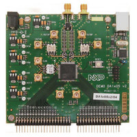
DAC1405D750/DB,598 NXP Semiconductors, DAC1405D750/DB,598 Datasheet - Page 25

DAC1405D750/DB,598
Manufacturer Part Number
DAC1405D750/DB,598
Description
BOARD DEMO FOR DAC1405D750
Manufacturer
NXP Semiconductors
Type
D/Ar
Datasheets
1.DAC1405D750HWC15.pdf
(42 pages)
2.HSDC-ACC01DB.pdf
(32 pages)
3.ADC1415S125DB598.pdf
(2 pages)
Specifications of DAC1405D750/DB,598
Number Of Dac's
2
Number Of Bits
14
Outputs And Type
2, Differential
Sampling Rate (per Second)
750M
Data Interface
Serial, SPI™
Settling Time
20ns
Dac Type
Current
Voltage Supply Source
Analog and Digital
Operating Temperature
-40°C ~ 85°C
Utilized Ic / Part
DAC1405D750
Product
Data Conversion Development Tools
Conversion Rate
750 MSPS
Resolution
14 bit
Interface Type
SMA
Supply Voltage (max)
3.3 V
Supply Voltage (min)
1.8 V
For Use With/related Products
DAC1405D750
Lead Free Status / RoHS Status
Lead free / RoHS Compliant
Lead Free Status / RoHS Status
Lead free / RoHS Compliant, Lead free / RoHS Compliant
Other names
568-5090
NXP Semiconductors
DAC1405D750
Product data sheet
10.5.1 Timing when using the internal PLL (PLL on)
10.5.2 Timing when using an external PLL (PLL off)
10.6 FIR filters
In
The setting applied to PLL_DIV[1:0] (register 02h[4:3]; see
map”) allows the frequency between the digital part and the DAC core to be adjusted.
Table 33.
The settings applied to DAC_CLK_DELAY[1:0] (register 02h[2:1]) and DAC_CLK_POL
(register 02h[0]), allow adjustment of the phase and polarity of the sampling clock. This
occurs at the input of the DAC core and depends mainly on the sampling frequency. Some
examples are given in
Table 34.
It is recommended that a delay of 280 ps is used on the internal digital clock (CLK
obtain optimum device performance up to750 Msps.
Table 35.
The DAC1405D750 integrates three selectable Finite Impulse Response (FIR) filters
which enables the device to use 4 or 8 interpolation rates. All three interpolation filters
have a stop-band attenuation of at least 80 dBc and a pass-band ripple of less than
0.0005 dB. The coefficients of the interpolation filters are given in
filter
Mode
Dual Port
Dual Port
Interleaved
Interleaved
Mode
Dual Port
Dual Port
Address
Dec
2
Fig 10. Input timing diagram when internal PLL bypassed (off)
Table 33
coefficients”.
(SYNCP − SYNCN)
Frequencies
Sample clock phase and polarity examples
Optimum external PLL timing settings
Q13 to Q0
“Frequencies”, the links between internal and external clocking are defined.
I13 to I0/
Hex
02h
SYNC
All information provided in this document is subject to legal disclaimers.
CLK input
(MHz)
185
92.5
370
185
Input data rate
(MHz)
92.5
92.5
Rev. 3 — 7 September 2010
Table 34 “Sample clock phase and polarity
Register name
PLLCFG
Input data rate
(MHz)
185
92.5
370
185
Dual 14-bit DAC, up to 750 Msps; 4 and 8 interpolating
90 %
t
Interpolation
4
8
su(i)
N
50 %
t
h(i)
90 %
280 ps
Value
Digital clock delay Bin
Interpolation
4
8
4
8
Update rate
(Msps)
370
740
N + 1
DAC1405D750
Table 9 “Register allocation
740
Update rate
(Msps)
740
740
740
DAC_CLK_
DELAY [1:0]
01
01
10001000
Table 36 “Interpolation
examples”.
© NXP B.V. 2010. All rights reserved.
N + 2
00 (/ 2)
01 (/ 4)
PLL_DIV[1:0]
01 (/ 4)
10 (/ 8)
Dec
136
DAC_CLK_
POL
0
0
001aal384
dig
88h
Hex
25 of 42
) to


