STEVAL-ILL021V1 STMicroelectronics, STEVAL-ILL021V1 Datasheet - Page 26
STEVAL-ILL021V1
Manufacturer Part Number
STEVAL-ILL021V1
Description
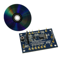
BOARD EVAL LCD BACKLIGHT LED7707
Manufacturer
STMicroelectronics
Specifications of STEVAL-ILL021V1
Design Resources
STEVAL-ILL021V1 Bill of Material STEVAL-ILL021V1 Schematic
Current - Output / Channel
85mA
Outputs And Type
6, Non-Isolated
Voltage - Output
36 V
Features
Dimmable, Extra 5V Output
Voltage - Input
4.5 ~ 36 V
Utilized Ic / Part
LED7707
Description/function
LCD backlight demonstration board
Operating Voltage
4.5 V to 36 V
Product
Display Modules
Core Chip
LED7707
No. Of Outputs
1
Output Voltage
36V
Dimming Control Type
PWM
Mcu Supported Families
LED7707
Lead Free Status / RoHS Status
Lead free by exemption / RoHS compliant by exemption
For Use With/related Products
LED7707
Other names
497-10044
Available stocks
Company
Part Number
Manufacturer
Quantity
Price
Company:

Part Number:
STEVAL-ILL021V1
Manufacturer:
STMicroelectronics
Quantity:
1


Application information
26/47
Equation 13b
Where V
Note that, the lower the inductor value (and the higher the switching frequency), the higher
the bandwidth can be achieved. The output capacitor is directly involved in the loop of the
boost converter and must be large enough to avoid excessive output voltage drop in case of
a sudden line transition from the maximum to the minimum input voltages.
However a more significant requirement concerns the output voltage ripple.
The output capacitor should be chosen in accordance with the following expression:
Equation 14
where ΔV
inductor current, T
Section 6.4.4 on page 33
Once the output capacitor has been chosen, the R
Equation 15
Where GM = 2.7 S and g
Equation 15 places the loop bandwidth at f
place the frequency of the compensation zero 5 times lower than the loop bandwidth:
Equation 16
Where f
In most of the applications an experimental approach is also very valid to compensate the
circuit. A simple technique to optimize different applications is to choose C
and to replace R
transient response. Insufficient damping will result in excessive ringing at the output and
poor phase margin.
Figure 18
Z
IN,min
OUT, max
= f
(a and b) give an example of compensation adjustment for a typical application.
U
/5.
is the minimum input voltage and I
COMP
is the maximum acceptable output voltage ripple, I
OFF
is the off-time of the switching cycle (for an extensive explanation see
with a 10 kΩ trimmer adjusting its value to properly damp the output
).
EA
= 375 µS
C
OUT
C
R
COMP
COMP
>
(
I
R =
, L
=
=
peak
U
2
2
. Then, the C
G
⋅ π
Δ ⋅
V
I
2
OUT
M
OUT
−
⋅ π
V
f
Z
I
⋅
OUT
OUT
OUT
g
⋅
f
1
U
COMP
R
EA
,
⋅
COMP
max
)
is the overall output current.
C
⋅
⋅
T
M
OFF
can be calculated as:
COMP
capacitor is determined to
L, peak
COMP
is the peak
= 4.7 nF
LED7707
Related parts for STEVAL-ILL021V1
Image
Part Number
Description
Manufacturer
Datasheet
Request
R

Part Number:
Description:
BOARD EVAL FOR MEMS SENSORS
Manufacturer:
STMicroelectronics
Datasheet:

Part Number:
Description:
KIT DEV STARTER ST10F276Z5
Manufacturer:
STMicroelectronics
Datasheet:

Part Number:
Description:
BOARD EVAL HDMI $ VIDEO SWITCH
Manufacturer:
STMicroelectronics
Datasheet:

Part Number:
Description:
BOARD DEMO ACCELEROMETER DIL24
Manufacturer:
STMicroelectronics
Datasheet:

Part Number:
Description:
BOARD STLM75/STDS75/ST72F651
Manufacturer:
STMicroelectronics
Datasheet:

Part Number:
Description:
EVAL BOARD 3AXIS MEMS ACCELLRMTR
Manufacturer:
STMicroelectronics
Datasheet:

Part Number:
Description:
BOARD EVAL 8BIT MICRO + TDE1708
Manufacturer:
STMicroelectronics
Datasheet:

Part Number:
Description:
EVAL BOARD A/D TS4657
Manufacturer:
STMicroelectronics
Datasheet:

Part Number:
Description:
BOARD ADAPTER 20DIP LIS3LV02DL
Manufacturer:
STMicroelectronics
Datasheet:

Part Number:
Description:
BOARD DEMO STM8S207R6/LIS331DLH
Manufacturer:
STMicroelectronics
Datasheet:

Part Number:
Description:
STMicroelectronics [RIPPLE-CARRY BINARY COUNTER/DIVIDERS]
Manufacturer:
STMicroelectronics
Datasheet:
Part Number:
Description:
STMicroelectronics [LIQUID-CRYSTAL DISPLAY DRIVERS]
Manufacturer:
STMicroelectronics
Datasheet:
Part Number:
Description:
BOARD EVAL FOR MEMS SENSORS
Manufacturer:
STMicroelectronics
Datasheet: