P0528 Terasic Technologies Inc, P0528 Datasheet - Page 34
P0528
Manufacturer Part Number
P0528
Description
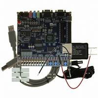
BOARD DEV DE1 ALTERA
Manufacturer
Terasic Technologies Inc
Type
FPGAr
Datasheet
1.P0528.pdf
(56 pages)
Specifications of P0528
Contents
DE1 Board, Power Supply, USB Cable, Plastic cover and software
For Use With/related Products
Cyclone II 2C20
For Use With
P0033 - BOARD ADAPTER HSMC TO GPIOP0006 - BOARD ADAPTER THDB-SUMP0001 - MODULE DIGITAL CAMERA 5MP (D5M)P0307 - KIT DEV 4.3" LCD TOUCH PANEL
Lead Free Status / RoHS Status
Lead free / RoHS Compliant
Other names
DE1


4.5 Using the Expansion Header
The DE1 Board provides two 40-pin expansion headers. Each header connects directly to 36 pins on
the Cyclone II FPGA, and also provides DC +5V (VCC5), DC +3.3V (VCC33), and two GND pins.
Figure 4.10 shows the related schematics. Each pin on the expansion headers is connected to a
resistor that provide protection from high and low voltages. The figure shows the protection
circuitry for only four of the pins on each header, but this circuitry is included for all 72 data pins.
Table 4.7 gives the pin assignments.
Signal Name
EXT_CLOCK
CLOCK_27
CLOCK_50
CLOCK_24
Figure 4.8. Schematic diagram of the clock circuit.
Table 4.5. Pin assignments for the clock inputs.
PIN_D12, PIN_E12
PIN_A12, PIN_B12
FPGA Pin No.
PIN_M21
PIN_L1
32
24 MHz clock input from USB Blaster
External (SMA) clock input
27 MHz clock input
50 MHz clock input
Description
DE1 User Manual
Related parts for P0528
Image
Part Number
Description
Manufacturer
Datasheet
Request
R

Part Number:
Description:
MODULE DIGITAL CAMERA 5MP (D5M)
Manufacturer:
Terasic Technologies Inc
Datasheet:

Part Number:
Description:
DE2-70 CALL FOR ACADEMIC PRICING
Manufacturer:
Terasic Technologies Inc
Datasheet:

Part Number:
Description:
USB BLASTER CABLE
Manufacturer:
Terasic Technologies Inc
Datasheet:

Part Number:
Description:
BOARD ADAPTER HSMC TO GPIO
Manufacturer:
Terasic Technologies Inc
Datasheet:

Part Number:
Description:
BOARD ADAPTER THDB-SUM
Manufacturer:
Terasic Technologies Inc
Datasheet:

Part Number:
Description:
KIT DEV 4.3" LCD TOUCH PANEL
Manufacturer:
Terasic Technologies Inc
Datasheet:

Part Number:
Description:
DAUGHTER BOARD AD/DA GPIO ADA
Manufacturer:
Terasic Technologies Inc

Part Number:
Description:
DAUGHTER BOARD AD/DA HSMC ADA
Manufacturer:
Terasic Technologies Inc

Part Number:
Description:
KIT MAX II MICRO
Manufacturer:
Terasic Technologies Inc
Datasheet:

Part Number:
Description:
BOARD DEV/EDUCATION ALTERA DE0
Manufacturer:
Terasic Technologies Inc
Datasheet:

Part Number:
Description:
DE2 CALL FOR ACADEMIC PRICING
Manufacturer:
Terasic Technologies Inc

Part Number:
Description:
MODULE DIGITAL CAMERA 1.3MP
Manufacturer:
Terasic Technologies Inc
Datasheet:

Part Number:
Description:
SENSOR CMOS 1.3MEGA (FOR P0349)
Manufacturer:
Terasic Technologies Inc
Datasheet:
Part Number:
Description:
MODULE DIGITAL CAMERA 5MP (D5M)
Manufacturer:
Terasic Technologies Inc
Datasheet: