C8051F800DK Silicon Laboratories Inc, C8051F800DK Datasheet - Page 143
C8051F800DK
Manufacturer Part Number
C8051F800DK
Description
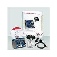
KIT DEV C8051F800
Manufacturer
Silicon Laboratories Inc
Type
MCUr
Specifications of C8051F800DK
Contents
Board, Cables, CD, Debugger, Power Supply
Processor To Be Evaluated
C8051F800
Data Bus Width
16 bit
Interface Type
USB
Operating Supply Voltage
7 V to 15 V
Lead Free Status / RoHS Status
Contains lead / RoHS non-compliant
For Use With/related Products
C8051F8xx
Lead Free Status / Rohs Status
Supplier Unconfirmed
Other names
336-1797


C8051F80x-83x
23.3. Priority Crossbar Decoder
The Priority Crossbar Decoder assigns a priority to each I/O function, starting at the top with UART0. When
a digital resource is selected, the least-significant unassigned Port pin is assigned to that resource (exclud-
ing UART0, which is always at pins 4 and 5). If a Port pin is assigned, the Crossbar skips that pin when
assigning the next selected resource. Additionally, the Crossbar will skip Port pins whose associated bits in
the PnSKIP registers are set. The PnSKIP registers allow software to skip Port pins that are to be used for
analog input, dedicated functions, or GPIO.
Because of the nature of the Priority Crossbar Decoder, not all peripherals can be located on all port pins.
Figure 23.4 maps peripherals to the potential port pins on which the peripheral I/O can appear.
Important Note on Crossbar Configuration: If a Port pin is claimed by a peripheral without use of the
Crossbar, its corresponding PnSKIP bit should be set. This applies to P0.0 if VREF is used, P0.1 if AGND
is used, P0.3 and/or P0.2 if the external oscillator circuit is enabled, P0.6 if the ADC is configured to use
the external conversion start signal (CNVSTR), and any selected ADC, Comparator, or Capacitive Sense
inputs. The Crossbar skips selected pins as if they were already assigned, and moves to the next unas-
signed pin.
Registers XBR0, XBR1, and XBR2 are used to assign the digital I/O resources to the physical I/O Port
pins. Note that when the SMBus is selected, the Crossbar assigns both pins associated with the SMBus
(SDA and SCL); when a UART is selected, the Crossbar assigns both pins associated with the UART (TX
and RX). UART0 pin assignments are fixed for bootloading purposes: UART TX0 is always assigned to
P0.4; UART RX0 is always assigned to P0.5. Standard Port I/Os appear contiguously after the prioritized
functions have been assigned.
Important Note: The SPI can be operated in either 3-wire or 4-wire modes, depending on the state of the
NSSMD1–NSSMD0 bits in register SPI0CN. According to the SPI mode, the NSS signal may or may not
be routed to a Port pin.
Rev. 1.0
143
Related parts for C8051F800DK
Image
Part Number
Description
Manufacturer
Datasheet
Request
R

Part Number:
Description:
SMD/C°/SINGLE-ENDED OUTPUT SILICON OSCILLATOR
Manufacturer:
Silicon Laboratories Inc
Part Number:
Description:
Manufacturer:
Silicon Laboratories Inc
Datasheet:
Part Number:
Description:
N/A N/A/SI4010 AES KEYFOB DEMO WITH LCD RX
Manufacturer:
Silicon Laboratories Inc
Datasheet:
Part Number:
Description:
N/A N/A/SI4010 SIMPLIFIED KEY FOB DEMO WITH LED RX
Manufacturer:
Silicon Laboratories Inc
Datasheet:
Part Number:
Description:
N/A/-40 TO 85 OC/EZLINK MODULE; F930/4432 HIGH BAND (REV E/B1)
Manufacturer:
Silicon Laboratories Inc
Part Number:
Description:
EZLink Module; F930/4432 Low Band (rev e/B1)
Manufacturer:
Silicon Laboratories Inc
Part Number:
Description:
I°/4460 10 DBM RADIO TEST CARD 434 MHZ
Manufacturer:
Silicon Laboratories Inc
Part Number:
Description:
I°/4461 14 DBM RADIO TEST CARD 868 MHZ
Manufacturer:
Silicon Laboratories Inc
Part Number:
Description:
I°/4463 20 DBM RFSWITCH RADIO TEST CARD 460 MHZ
Manufacturer:
Silicon Laboratories Inc
Part Number:
Description:
I°/4463 20 DBM RADIO TEST CARD 868 MHZ
Manufacturer:
Silicon Laboratories Inc
Part Number:
Description:
I°/4463 27 DBM RADIO TEST CARD 868 MHZ
Manufacturer:
Silicon Laboratories Inc
Part Number:
Description:
I°/4463 SKYWORKS 30 DBM RADIO TEST CARD 915 MHZ
Manufacturer:
Silicon Laboratories Inc
Part Number:
Description:
N/A N/A/-40 TO 85 OC/4463 RFMD 30 DBM RADIO TEST CARD 915 MHZ
Manufacturer:
Silicon Laboratories Inc
Part Number:
Description:
I°/4463 20 DBM RADIO TEST CARD 169 MHZ
Manufacturer:
Silicon Laboratories Inc